
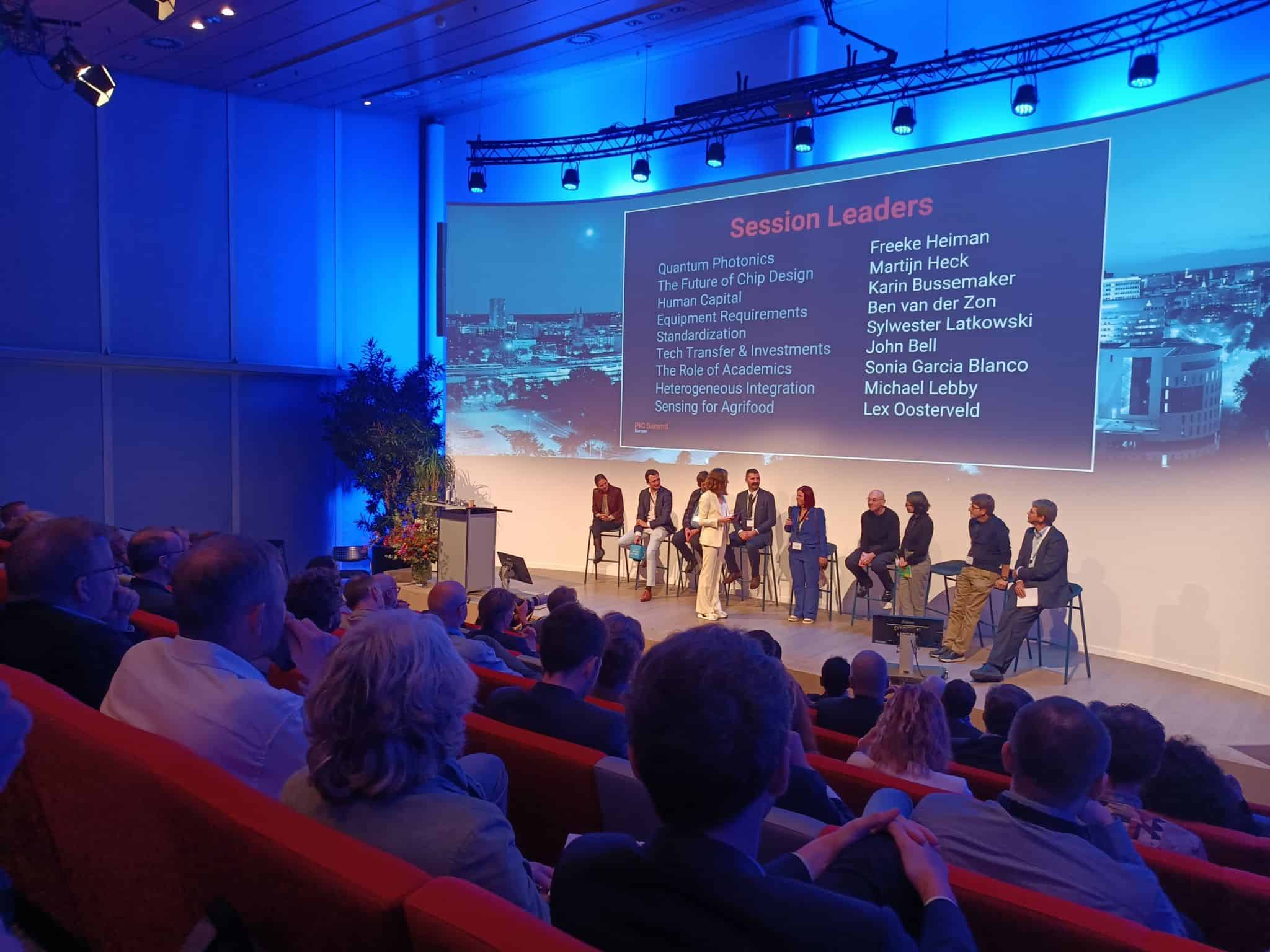
Two panel sessions during this year’s PIC Summit Europe 2022 were devoted to the heterogeneous integrations between various parts of electronics and photonics. Expertise from all corners of the value chain was brought together to find out about the current state of the industry, as far as co-design, co-simulation, and co-production of electronic and photonic circuits are concerned.
With the growing maturity of fabrication processes for PICs, true process design kits are now being set up which include process statistics that allow design for manufacturability. In addition, there’s a growing convergence with electronic design tools, for co-simulation. These trends open up new directions for the field. Additionally, the increasing global demand for communication and computing technology puts pressure on chip manufacturers. The industry is aware that monolithic technology alone is not enough to handle that pressure. The answers are sought in a smart combination of materials, and both photonic and electronic circuitry. The field of heterogeneous integration is exploring techniques like ‘die and wafer bonding’, and ‘micro-transfer printing’.
Many sideways
What does this entail? What does the future hold for photonic and electronic co-design? Well, the industry is not sure yet. Those who watched the sessions – led by Martijn Heck of TU Eindhoven and Michael Lebby of Lightwave Logic – found themselves in a very nuanced place. Yes, we’re on our way, but the road ahead still has many sideways. “And we will decide which path to choose along the way.”
Mixing and matching are already here, Michael Lebby concluded. “It’s going to happen, if only because the industry will keep looking for better performances. But there are many approaches, many applications, many combinations – we still have to sort out which will be most effective. We can be certain that there’s a whole bunch of opportunities that will use a whole bunch of combinations.”

For Martijn Heck, it was hard to formulate a key takeaway from his session. “What we discussed is more of an assessment than it would be a takeaway: we are moving forward together, and we have a common goal, but we need more time to find out what the ideal road to success exactly looks like. So I would like to ask the whole photonics community to engage with us to assess where we are at the moment and how we can find the best road ahead.”
The scattered views also became clear when Mr. Heck asked the audience to join the discussion. “How do you think electronics and photonics will go together in one system”, he wanted to know. “Do you see a solution in multiple dies (chips) assembled together with flip-chip or wire-bond approaches, in more heterogeneous approaches, using micro-transfer printing, die and wafer bonding, or rather in monolithic solutions where electronics and photonics are fabricated on the same substrate?” Dozens of hands went in the air for every one of the potential answers. Plus the suggestion for another option: “All of the above.”
Designing a product
The audience’s view was exemplary for the discussion within the two panels. Packaging was positioned as a good option for integration, as was an interface to communicate between systems. What the panels did agree upon is that it all comes down to the actual use: the functions and applications will be decisive for the way the integration process will proceed. “This is about designing a product, not a chip”, Katarzyna Lawnizcuk (Bright Photonics) said.
Another point of agreement was in the complexity of the circumstances around the integration initiatives. “The electronics and photonics communities still are mostly separate worlds, with the latter far less mature than the first, but you have to solve everything simultaneously.” Bridging those communities is one of the big tasks for now, but even so, Lebby remained assured: “It’s going to happen.”
PIC Summit Europe 2022 is a new congress, one of two photonic chip conferences in Europe and will return annually. It is expected to take place again next year in November. PhotonDelta is the lead organizer of the congress; the program was set up together with the Eindhoven University of Technology and IPSR-I.
Collaboration
Related Posts


