Dutch Scientists have unveiled a ground-breaking self-organisation strategy, Reaction-Diffusion Driven, Immersion-Controlled Patterning (R-DIP). A new way to pattern thin films. They published their findings in Advanced Materials. The method, using immersion-controlled reaction-diffusion, crafts complex line motifs, bringing a new level of precision and control to thin film patterning. Its potential is enormous: from creating wafer-scale diffraction gratings to opto-mechanical sensors based on Moiré patterning, R-DIP’s versatility is evident. R-DIP could offer a cost-effective and scalable alternative to traditional lithography techniques, driving significant advancements in the production of optical, electronic, and mechanical devices.
- Dutch Scientists introduce Reaction-Diffusion Driven, Immersion-Controlled Patterning (R-DIP) for precise thin film patterning.
- R-DIP employs immersion-controlled reaction-diffusion to create uniform line patterns with tunable spacing and error-correction capabilities.
- R-DIP shows potential as a cost-effective alternative to traditional lithography, enabling intricate device manufacturing and driving materials science advancements.
Unravelling the Intricacies of R-DIP
At its core, R-DIP is a self-organization strategy that uses immersion-controlled reaction-diffusion to create specific line patterns on thin films. The process involves putting a gel film with one substance into a liquid solution with another substance. This starts a reaction when they touch, which makes even patterns on the gel. In simpler terms, when the gel touches the liquid, a reaction occurs that makes neat lines on the gel.
One important aspect of R-DIP is its ability to change how fast the gel goes into the liquid. This controls how the reaction spreads across the gel. As a result, it makes very even lines where the reaction happens. By adjusting the speed and how the reaction moves, it’s possible to create patterns with exact spaces between the lines. This means the operator has control over what pattern shows up.
The Versatility of R-DIP
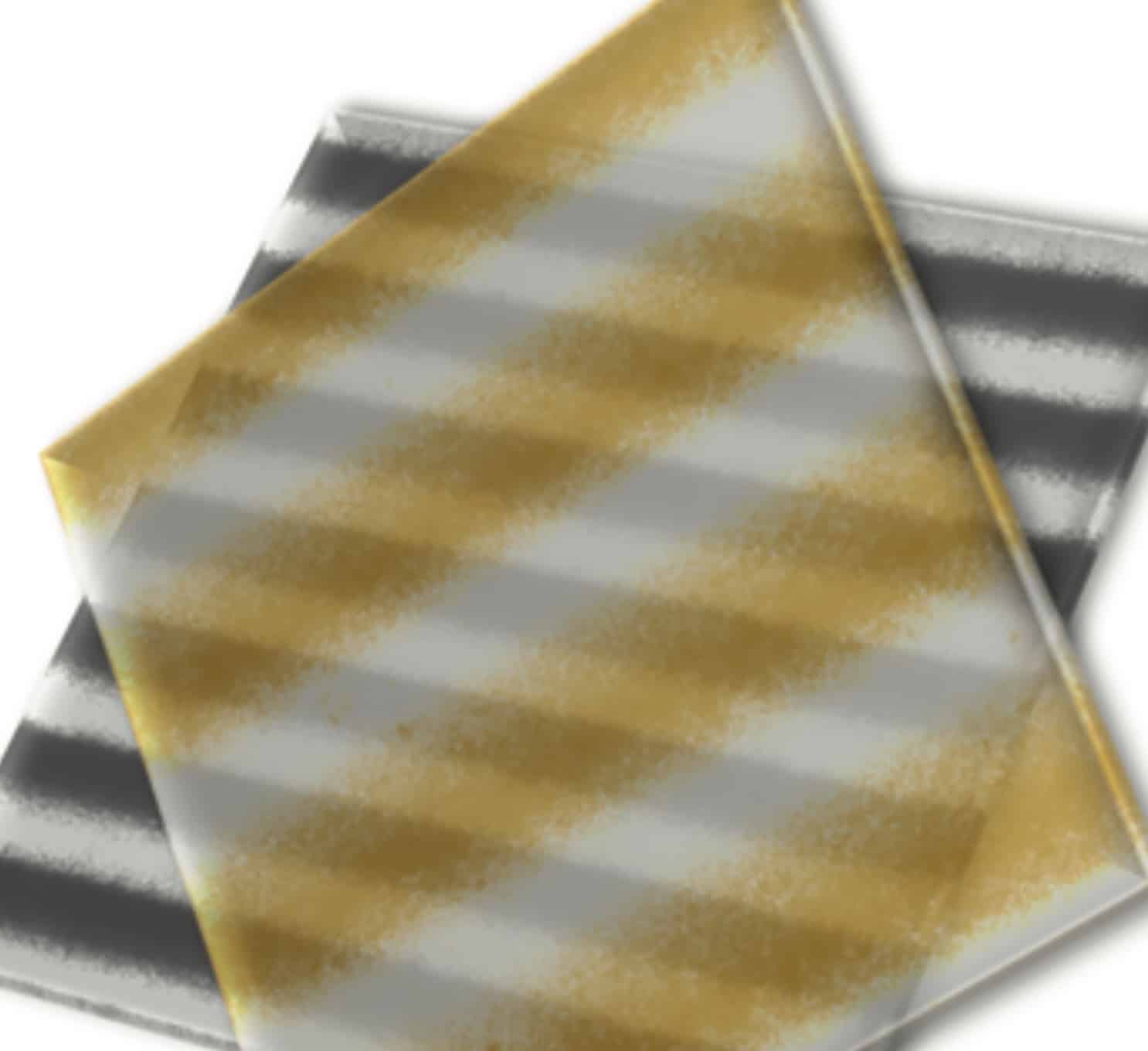
The R-DIP method is not limited to a single type of material or pattern. It has been demonstrated using various materials, including silver/silver oxide nanoparticles, silver chromate, silver dichromate, and lead carbonate, to manufacture line patterns. By combinatorially stacking different line patterns, hybrid materials with multi-dimensional patterns, such as square, diamond, rectangle, and triangle motifs, can be fabricated.
Beyond its versatility in materials and patterns, R-DIP also offers error-correction against defects, supporting the sustenance of uniform micro-scale ordering over long distances. This capability is particularly relevant in the production of wafer-scale diffraction gratings and opto-mechanical sensors based on Moiré patterning, showcasing R-DIP’s functionality potential and scalability.
Implications for Lithography
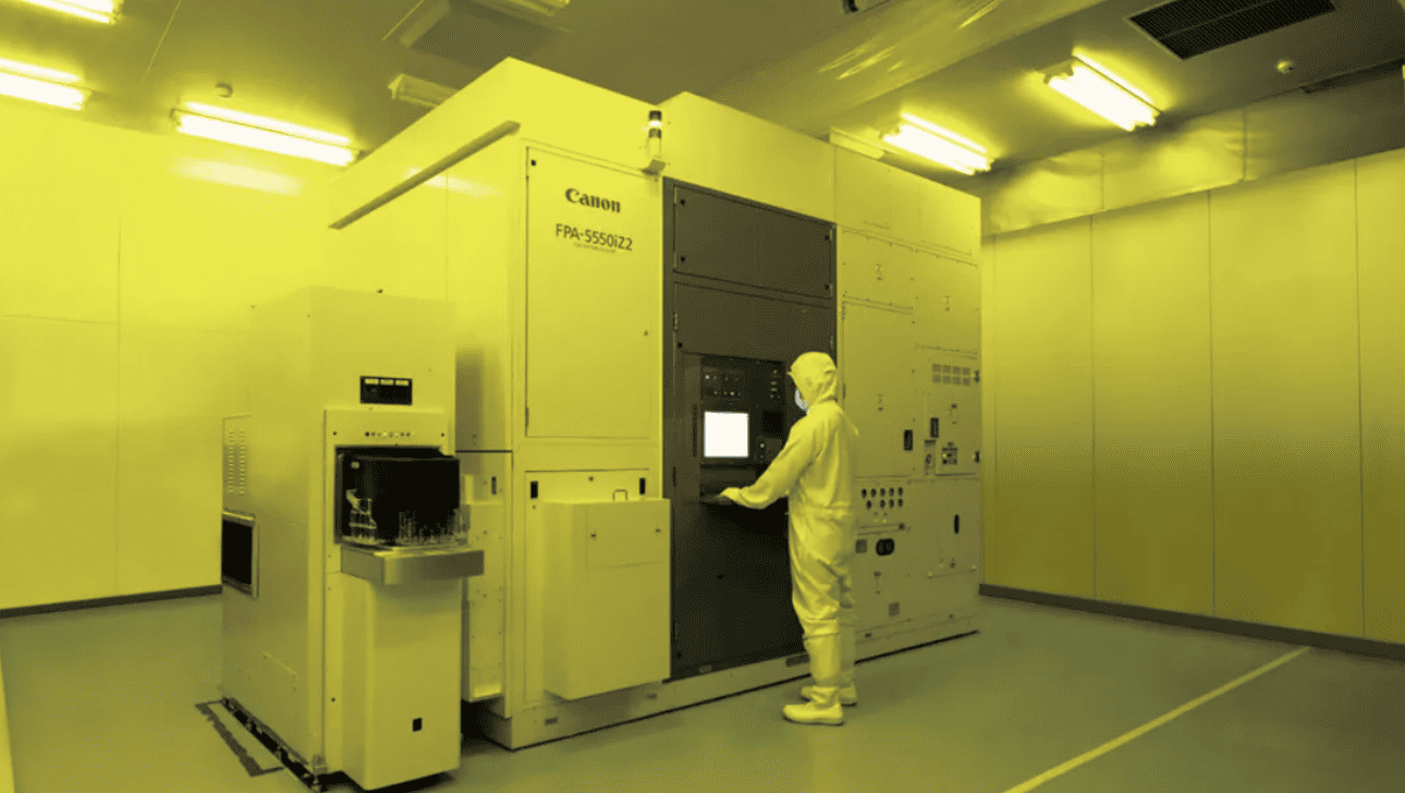
R-DIP might impact lithography processes, such as those used by ASML. Lithography, a critical step in the computer chip-making process, involves coating a wafer with photosensitive material and exposing it to light. This process, while effective, is costly and requires sophisticated machinery.

R-DIP, with its autonomous and scalable nature, offers a potential alternative to these costly lithography techniques for producing nanoscale complexity in thin films. The ability to produce complex line motifs with tunable line spacing and error-correction against defects could be a game-changer in the manufacturing of intricate devices, including computer chips.
As with any new technology, there are likely to be challenges and limitations associated with the implementation of R-DIP. These may include equipment costs, the need for highly skilled operators, and potential environmental implications associated with the use of certain reagents. It is anticipated that the further development and refinement of R-DIP will continue to drive advancements in the production of optical, electronic, and mechanical devices.


