
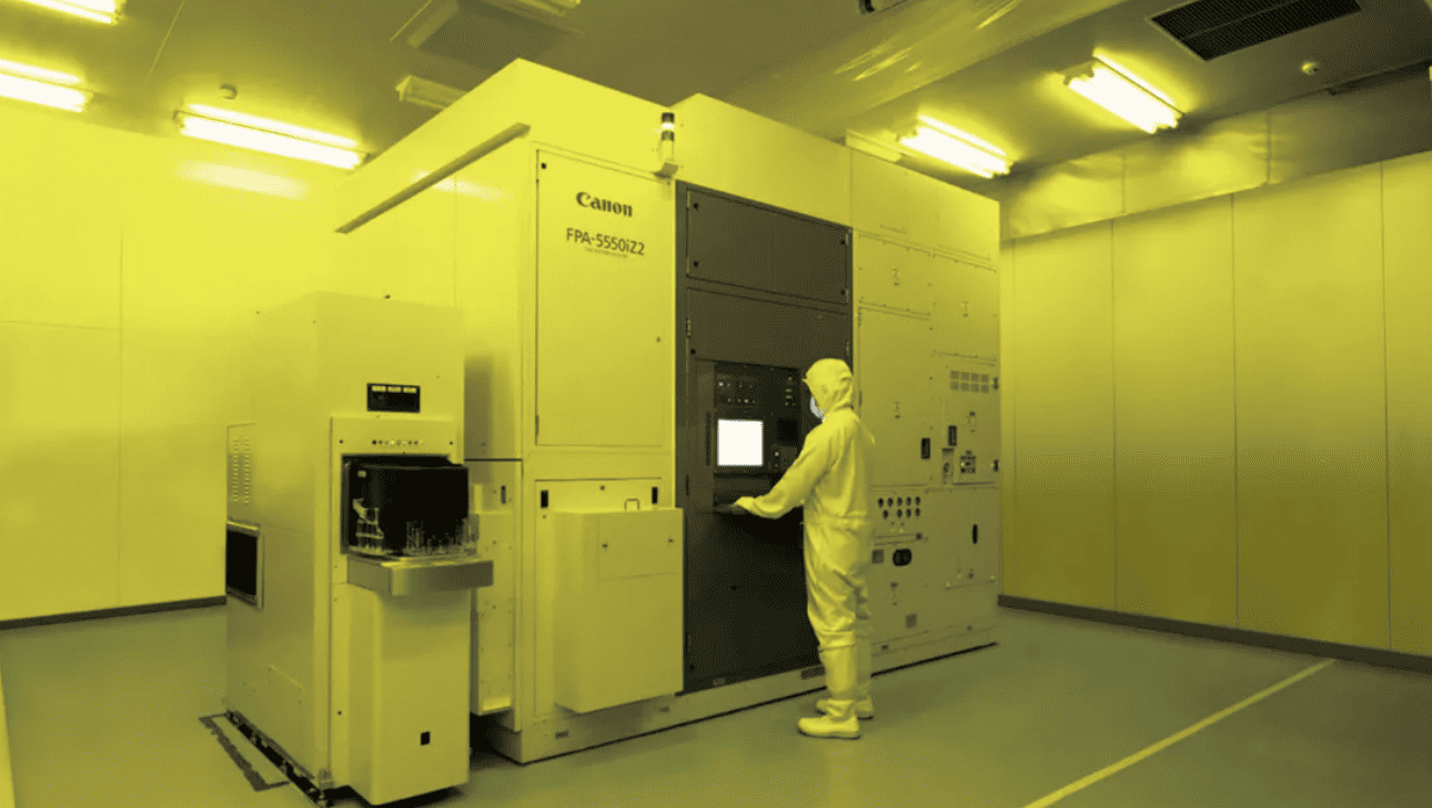

Canon, a household name for its cameras, is making waves in the semiconductor industry with its newly launched FPA-1200NZ2C nanoimprint lithography system. This innovative technology is dubbed a potential game-changer, “challenging the dominance of optical lithography and offering high resolution, cost efficiency, and adaptability in the ever-evolving semiconductor manufacturing arena”. Despite its slower speed and certain limitations, Canon’s equipment shows promise in specific applications such as 3D NAND memory, photonics, biochips, and microfluidics. But more is needed to become a threat to ASML’s dominance in the industry.
Capabilities
First, let’s take a look at its capabilities, as announced by Canon itself. With an ability to manufacture semiconductors equivalent to a 5nm process and as small as 2nm, it surpasses the capabilities of ASML’s machines. Also, Canon’s system reduces power consumption, contributing to CO2 reduction, and aligns with the growing demand for energy-efficient technology. This development signals Canon’s strategic shift to the semiconductor supply chain.

In contrast to conventional photolithography equipment, which transfers a circuit pattern by projecting it onto the resist-coated wafer, the new product does it by pressing a mask imprinted with the circuit pattern on the resist on the wafer like a stamp, Canon says. “Because its circuit pattern transfer process does not go through an optical mechanism, fine circuit patterns on the mask can be faithfully reproduced on the wafer. Thus, complex two- or three-dimensional circuit patterns can be formed in a single imprint, which may reduce the cost of ownership.”
Canon’s entry into the semiconductor industry follows its acquisition of Molecular Imprints Inc., a company focused on advancing nanoimprint lithography technology. This strategic acquisition bolsters Canon’s technological arsenal, enabling it to develop a system that competes with industry leaders ASML and Nikon.

A threat to optical lithography? Maybe not so much
Canon’s implementation of nanoimprint lithography (NIL) technology is widely seen as a potential threat to the dominance of optical lithography in the semiconductor manufacturing industry. But is it? Not really, ASML’s Sander Hofman writes in his weekly newsletter Always Be Curious. “The big drawbacks are that this mechanical manufacturing process is slow and inherently causes micro-distortions on the wafer. This affects alignment between subsequent layers in a chip and causes defectivity. This means bad chips and general yield loss at lower productivity, a chipmaker’s worst nightmare.”

In today’s integrated circuitry, which generally consists of dozens of layers stacked with nanometer accuracy, Hofman adds that this has long been the key hurdle for nanoimprint lithography. “And even though Canon has painstakingly improved alignment with hardware and software innovations over the last few years, the semiconductor industry is organized around specific lithographic requirements and process flows that are optimized for mass production, so it is biased to invest in the proven infrastructure that minimizes risk, time, cost and complexity, yet maximizes productivity. Nanoimprint lithography’s remaining challenges mean that it simply doesn’t play a similar role as optical lithography in the mass production of the world’s most advanced chips.”
Other markets
Canon will focus on other markets, Hofman expects. “Canon has taken nanoimprint farther than ever before, and it’s now becoming an interesting technology for specific semiconductor manufacturing cases, like in 3D NAND memory (which has more relaxed defectivity requirements and leverages the system’s ability to more freely sculpt 3D structures) and in photonics (which needs high-resolution structures with high reproducibility and scalability on different substrates, without the challenge of alignment). And there are more new applications on the horizon that might benefit from nanoimprint lithography, such as biochips and microfluidics.”
Related Posts


