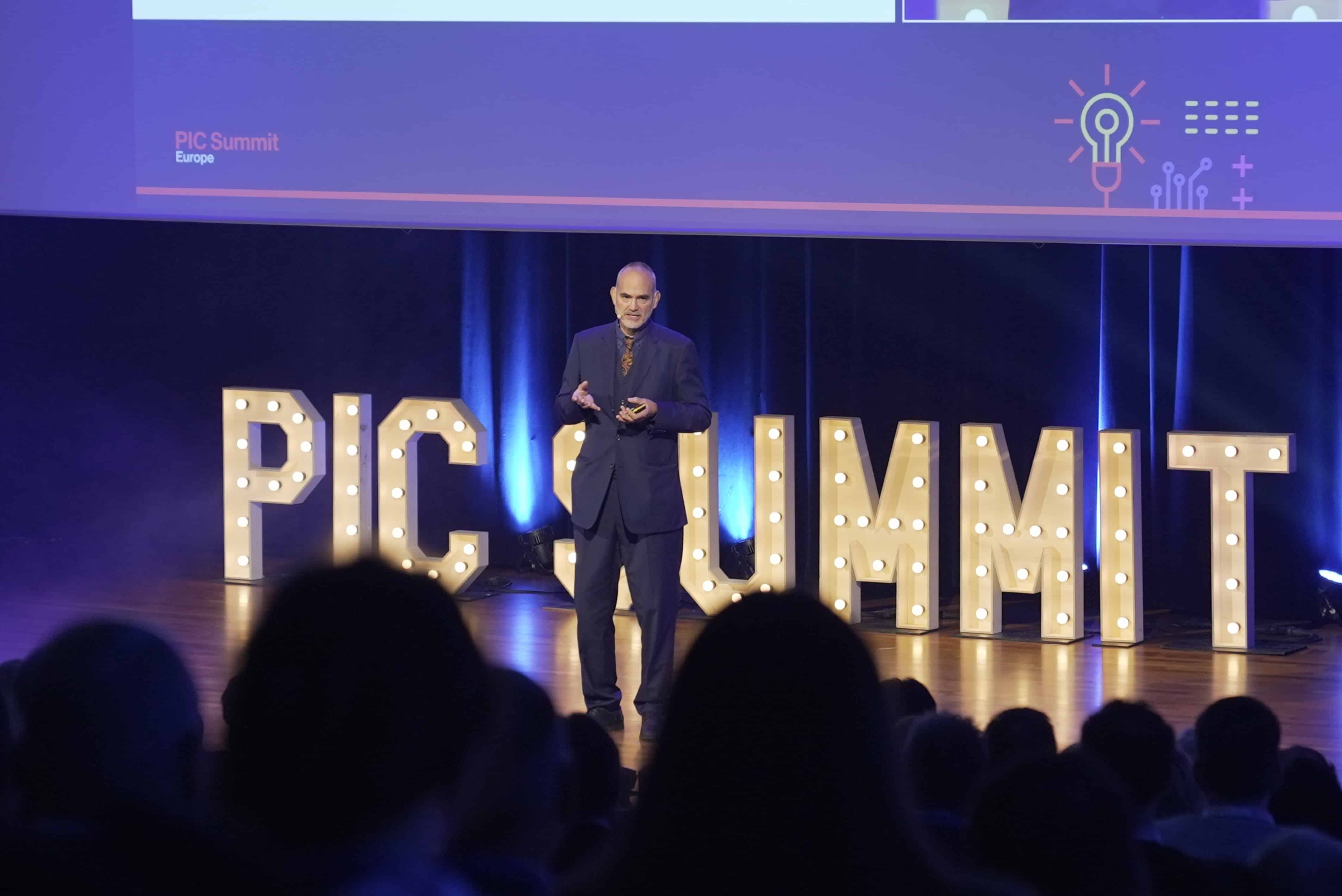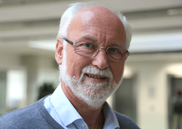
Meint K. Smit has been given a life-time achievement award in recognition of his contributions to the development of a vibrant Indium Phosphide PIC ecosystem in Europe. He was recognised by international leaders in the Photonics Industry. The PIC Awards are an initiative of PIC International, the leading conference and journal specialising in next generation photonic integrated circuits. Thousands of votes were received, with the results being announced in Brussels on March 7th 2017.
Jonathan Marks took the opportunity to find out more about Meint Smit and his passion for optics and nanotechnologies. In this profile, he discusses what’s coming next and why this phase is important for both research and industry.
The Story so far
“We’ve analysed the success of microelectronics. Now we’re putting those lessons learned to work for integrated photonics” says Professor Meint Smit of Eindhoven University of Technology.
The development of silicon based microelectronics means today it costs only a few cents to design and develop per square millimetre of chip, as the technology is mature and highly standardized. In addition, its development costs are low because we have sophisticated software for the fast and accurate design of the chips.
Teams at Eindhoven University of Technology (TU/e), led by Professor Meint Smit, want the same for photonic devices. And now that tipping point has been reached.
“Around the start of this new century, we were all asking ourselves: when is photonics integration really going to take off in the same way as silicon micro-electronics?” explains Smit. “After all, in 1980 I had started saying it would kick start in the 1990. Ten years later, the tipping point had moved to the start of the new millennium. By that time, some critics started to say that the promise of photonics integration would always remain in the future.”
Building on the success of microelectronics
“In Eindhoven, we looked at the world of microelectronics and discovered that things were arranged in a very different way. Up until the 1980’s a lot of different technologies were being used. There were a whole range of transistor types and countless variations between them. But in the 1980’s things started converging and you started to see the development of generic processes.”
“Designs start to use the same basic building blocks of transistors, resistors and capacitors. Even some of today’s most complicated processors, with over 1 billion transistors, have less than 10 different components. So, you are using the same set of building blocks to create all kinds of things.”
“We asked ourselves, how can this be applied to photonics? If you look to light, it has an amplitude, a phase and a polarisation. So, if you make a component for manipulating the amplitude, another one for altering the phase, and one for changing polarisation, you could achieve a lot of things. Then you simply need a waveguide to connect them.”
“So, we started developing a process with an optical amplifier for the amplitude, a phase modulator to change the phase, and a polarization converter.”
“There is a big advantage if everyone uses the same generic process. You can combine a lot of different designs on one chip. At the moment, we can put 20 different designs on one wafer. And that will increase as we start to use larger wafers in commercial production.”
There’s always more than one run
“The challenge in this business of integrated photonics has been the cost of making a chip prototype. If you develop a chip it always takes 2-3 runs before you get it right, because the chip never performs exactly as you expect.”
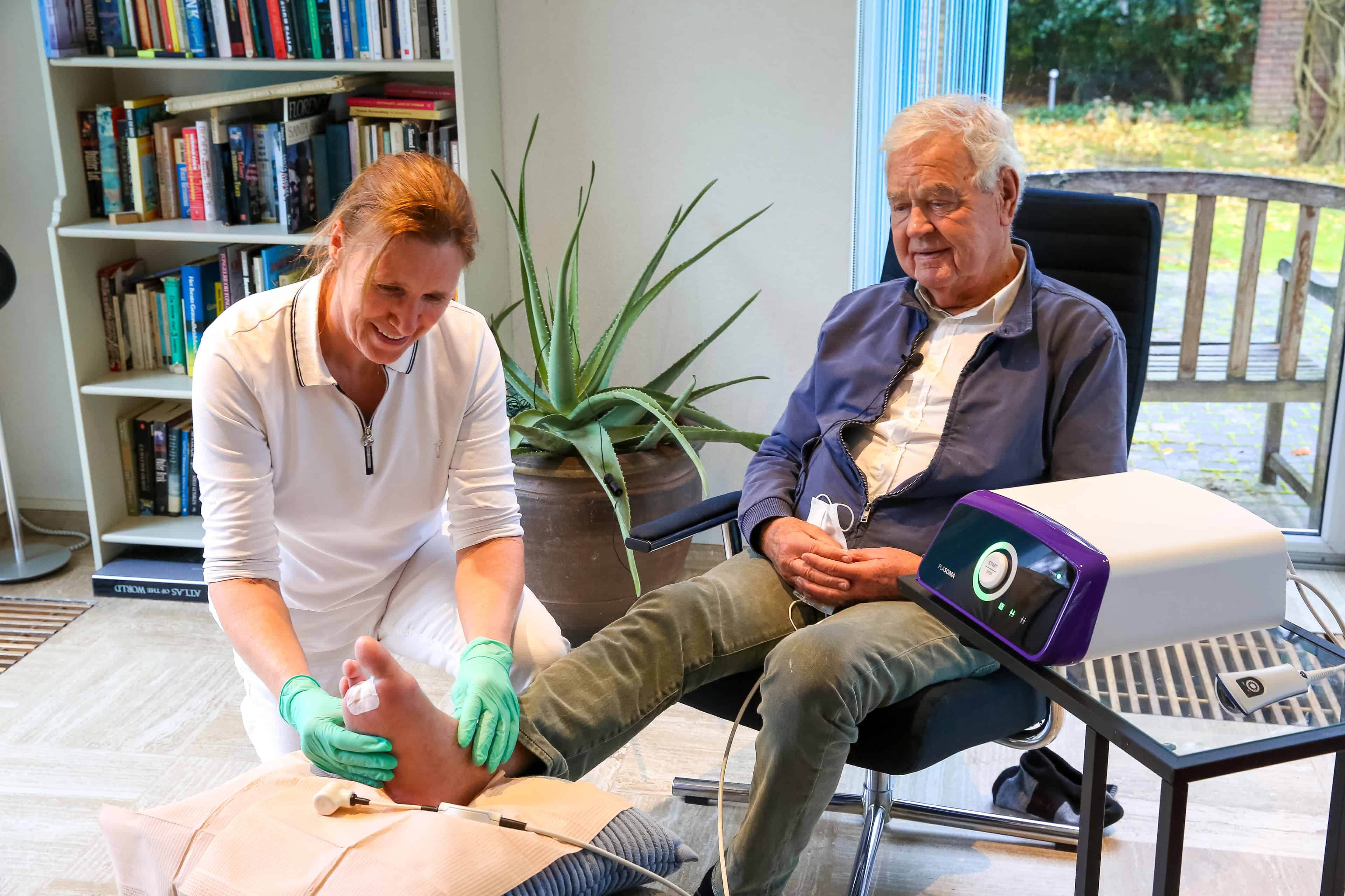
“Traditionally, one process run currently used to cost at least €200,000, if you do it on your own. This is a huge barrier for small companies. And when you know that 80% of Europe’s photonics companies are small/medium enterprises, then this used to be a problem. But if 20 users can share the same wafer, then the costs drop to below €10,000 each and that’s within the scope of many startups. You get 8 identical cells back from the foundry which you can test and measure. You can then iterate the design, so that the next run gives even better results.”
Open Collaboration is key to maintaining Europe’s Lead
Eindhoven Technical University (TU/e) also drives and actively contributes to the International JePPIX platform. This is an open collaboration between over 15 partners, most of them key-players in photonic integration, designed to connect researchers, PIC designers, and generic foundries to dramatically cut costs and speed up the time to market. TU/e have also been a partner in setting up Smart Photonics, to make its knowhow on generic Photonic IC fabrication available to users on a commercial basis.
“The role of JePPIX is to act as an independent broker between users, designers and foundry’s. We announce a production schedule, collect the designs and bring them together in one big mask set. That goes to the foundry that produces the wafers, dices them in separate chips and sends the chips to the various designers. This is the way TU/e has introduced generic photonics manufacture into Europe.”
The race is on
“Clearly, others have recognized we’re on to something. In October 2014, several leading universities and technology companies took part in the US tender to create the “Integrated Photonics Institute for Manufacturing Innovation”. In late July 2015, we learned that the winning bid was the city of Rochester. Additional private funding means a total of around US$610 million has been set aside to fund the US program in photonics chip manufacture. There are similar major investments being made in South Korea and China.”
“It turns out that the generic integration foundry infrastructure and logistics is quite complex, so being able to master this gives us a head start. Now we’ve reached a very important tipping point. And we are only at the beginning of what is possible.
When we look at the world of semiconductors, in the 1980s no-one thought such generic processes could ever drive very fast 60 GHz radio frequency circuits. Personally, I think if you are willing to invest enough money in a single technology, then it will surpass most of the other technologies.”
Indium Phosphide Wins on Price and Performance
“Now, let’s suppose your chip works and you’re happy with its performance. Then scaling up to produce 100,000 pieces is no problem. You can order them immediately knowing that the specs will remain constant.
“The other point is the chip cost. Many people think that InP is very expensive. In comparison with silicon fabs. We are actually less expensive for low and medium volumes, while at the same time offering excellent performance.
“Of course, silicon photonics can make their chips cheaper if you buy millions. But few small companies start with millions. They want to start with a few hundred or a few thousand. These volumes are too small for most silicon. Further, chip cost is usually only a small part of the total cost of assembling a module. Because InP enables integration of the full circuit in a single chip, including lasers and optical amplifiers, the assembly costs will be lower than for silicon, where you always have to assemble the lasers in a hybrid way. So, if you look at the functionality per Euro, Indium Phosphide wins and we are very competitive.”
“The next step that we are working on is to do the whole thing again but then not on a substrate of Indium Phosphide, but on a silicon wafer that has the electronics integrated to drive and control the photonic chip. But then we will add a very thin layer stack of Indium Phosphide.”
Riding the Seven League boots of Silicon
“The holy grail of this industry has been to put lasers onto a piece of Silicon. Silicon itself is not suitable for this – you can’t generate light directly, whereas with Indium Phosphide you can generate light directly in the chip. We are developing methods to build full photonic circuits in a thin Indium Phosphide layer on top of a silicon wafer containing the driver, receiver and control electronics, so that we get very short and efficient connections between the two. JEPPix is participating in the WIPE project, for instance, to do just that.”
“We think that Indium Phosphide will champion by applying the methodology of microelectronics to InP-based photonics and we believe our generic approach will show rapid scaling.”
Quick Questions to Meint
Meint K. Smit was born in Vlissingen, the Netherlands, in 1951. In 1974 he started work on radar and radar remote sensing, joining the Delft University of Technology in 1976. He switched to optical communications in 1981, becoming leader of the Photonic Integrated Circuits group at Delft University in 1994. He is the inventor of the Arrayed Waveguide Grating for which he received a LEOS Technical Achievement award in 1997. In 2002 he moved with his group to Eindhoven University of Technology, where he became leader of the Opto-Electronic Devices group within the Institute for Photonic Integration. In 2002 he was appointed LEOS Fellow for contributions in the field of Opto-Electronic Integration.
You started your career in radar and remote sensing. Why did you switch to integrated optics?
At that time, integrated optics was very new, while radar remote sensing was a mature technology, but less adventurous. I was attracted by the novelty, pioneering areas of research that had not yet been explored.
Will there be enough photonics engineers as the industry ramps up? Are Universities producing enough qualified students?
The answer is no, but we are doing our very best to educate more of them.
What is your preferred future for the photonics industry in Europe. What needs to happen so that it takes off faster?
It is a matter of investing in the whole ecosystem. That means in foundries to develop better foundry processes. In design software tools and so-called Process Design Kits to enable faster and better designs. In packaging and test facilities. And in programs to reach out to potential users and offer them low-cost opportunities for exploring what the technology can bring to their product portfolio.
What has been the highlight of your career so far?
I think that there are two highlights: the invention of the Arrayed Waveguide Grating and the introduction of generic foundry technology to Photonics.
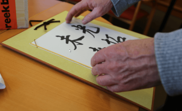
 What’s the story behind the Japanese kanji character on your office wall?
I got it from Prof. Utaka from Waseda University, who worked in our Lab for a few months. His hobby was calligraphy of Japanese characters. He gave it to me when he left our group. It means: Photonics lights the future.


