
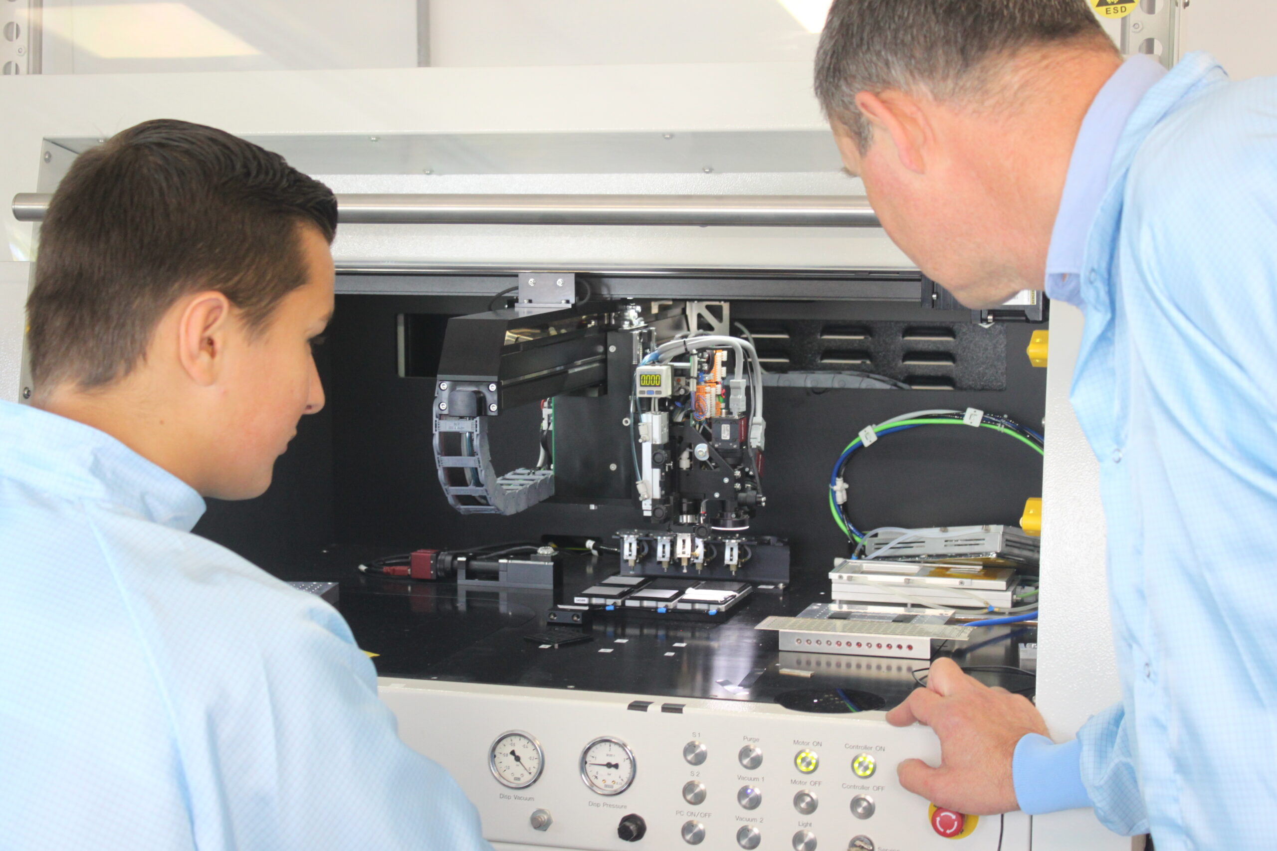

The Chip Integration Technology Center (CITC) and the HAN University of Applied Sciences (HAN) have jointly developed a new degree program that focuses entirely on the semiconductor industry. In recent years, Nijmegen and its surroundings have become a semiconductor hotspot, with many companies focusing on the development and manufacture of chips. “Partly because of that focus, requests are also coming in from companies for highly qualified personnel who know everything about chips and their casings,” says Joop Bruines, who works for both CITC and the HAN.
Several chip manufacturers have for some time had the ambition to train students up with the specialized knowledge from their fields. “The study program is tailored to the companies’ needs. In particular, there was no training available yet for the phase in which chips are packaged in their casings,” says Bruines. HAN and CITC have developed this minor In order to bridge this knowledge gap.
In-house talent
The open innovation center CITC in Nijmegen develops packaging and integration technology especially for chips. It was established in 2019 in collaboration with Delft University of Technology (TU Delft) and the Netherlands Organisation for Applied Scientific Research (TNO). At CITC, companies, research institutes and educational institutions get to work together. With the new program, companies such as NXP, Ampleon, Sencio, BESI or Nexperia can train and recruit new talent themselves.

Immediately employable
Chip packaging is becoming more and more complex. Developments like System-on-a-Chip and System-in-a-Package, embedded antennas, sensors and Microelectromechanical Systems, make heavy demands on the manufacturing process and on the skills of employees. Casings are becoming increasingly complex and application-specific, while costs have to remain low. Joep Stokkermans, Director Innovation Equipment & Automation Technologies at Nexperia says: “Nowadays, it often takes us two to three years to get a technology student completely familiarized with the material. The gap between study and work is too big.” In the new study course, students learn the most advanced techniques so that they will be immediately ready to start working.

International
Last year, seven part-time students had already started working while pursuing a minor. These were mainly employees in the semiconductor industry who wanted to specialize themselves further. The minor has since been expanded to a full-time version for the new academic year. Fourteen full-time students have registered who come from all over the Netherlands, some from Germany and even one from Finland. Among the students are also employees of companies that are not affiliated with CITC or HAN.
Also read: Sustainable chips: Wiring from gold to copper to … nothing?
Collaboration
Related Posts


