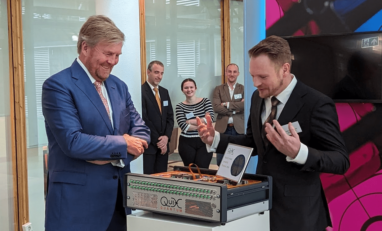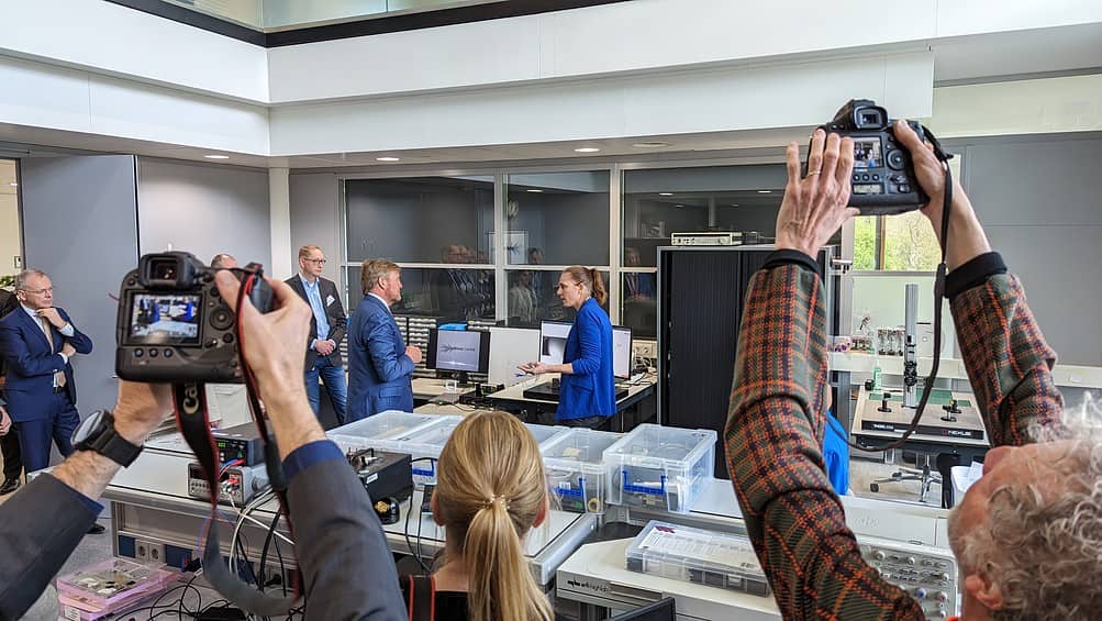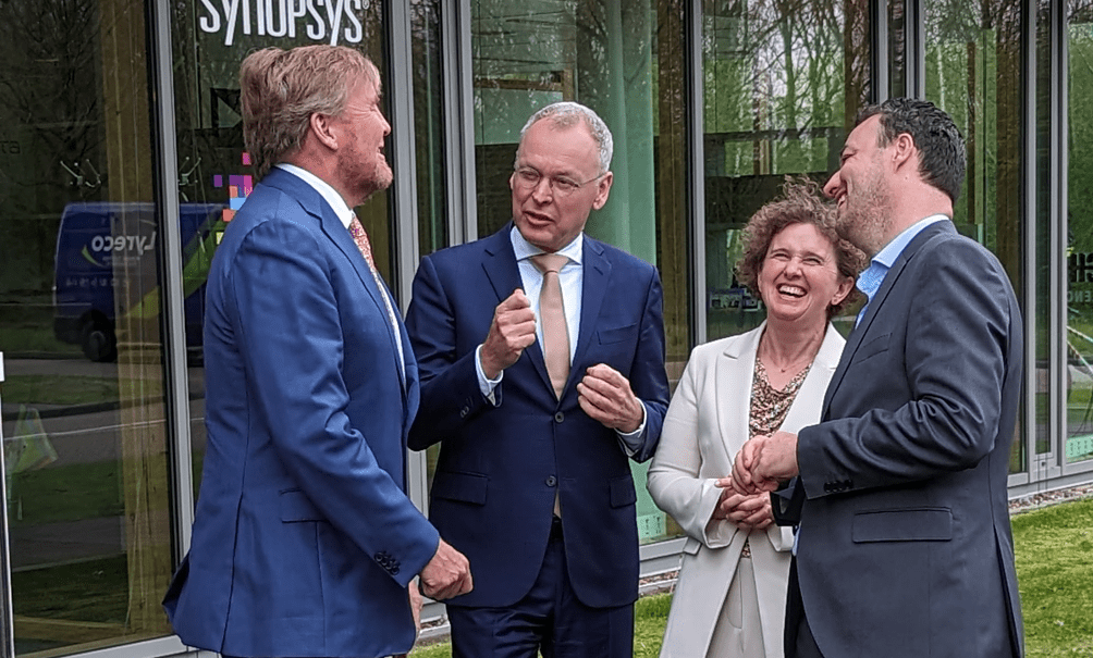
The strength of the Netherlands as a market maker, the importance of a European ecosystem, and a barrage of examples of applications that will define our world in the coming years. These were the main themes of today’s visit by a very interested King Willem-Alexander to the High Tech Campus in Eindhoven. Everything revolved around integrated photonics, the technology that is seen worldwide as decisive for the development of smaller, faster, and energy-efficient devices. With demonstrations at Holst Centre and roundtable discussions at PhotonDelta, the King learned about the essence of the technology, its applications, and its importance for the future of the Netherlands and Europe.
That the innovations shown will lead to applications that will help solve the great challenges of our time and contribute to a healthy and sustainable future, there was no misunderstanding about that during this visit. Markets that stand out most in this regard are those of medical diagnostics, autonomous driving, the agricultural sector and data communication. “The King’s visit once again underlines the importance of integrated photonics for our country,” PhotonDelta director Ewit Roos summed up the visit afterwards.
The King was updated on various applications, including lidar, lifi, quantum, and medical sensors. In addition, he was informed about the forces within the entire ecosystem, from chip design to production and marketing; the importance of good education – especially at the mbo level – was also given full attention. The King had prepared himself well, it turned out. His questions were to the point (What about the I.P.? How would you solve this without photonics? Where are the logical connections to the German industry? What is a bigger challenge now, money or people?) and led to animated conversations in the lab, at the roundtables, and at the demonstrations.

This emerging chip technology is accelerating thanks to a 1.1 billion euro program led by PhotonDelta. Ewit Roos: “The King’s visit is a huge honor for the entire ecosystem. PhotonDelta and Holst Centre are central to the development of this new value chain. For the King, this was certainly a wonderful opportunity to get the most complete picture possible of the quality of the unique position of the ecosystem and all the opportunities that still lie ahead.”
National Growth Fund
The Netherlands has recognized the opportunities of integrated photonics through the National Growth Fund. PhotonDelta, the ecosystem of organizations in photonic chip technology, has mobilized public and private investment totaling 1.1 billion euros through this fund to transform the Netherlands into a leader in the next generation of semiconductors. The investment consists of 470 million euros through the growth fund, with the rest coming from other partners and stakeholders. It is all part of the Dutch government’s plan to strengthen the country’s position as a world leader in integrated photonics.
Demonstrations and roundtable discussion
The King first visited Holst Centre, a collaboration between the research centers imec and TNO. Researchers from different disciplines develop new technology for photonic chips and prototypes that companies can use for their production process and new products.
The King was given a tour of Holst Centre’s laboratory and attended demonstrations of the application of photonics in various sectors. Representatives from Signify, Effect Photonics, Delta Diagnostics, Quix Quantum, and Lionix explained the different stages in the value chain. During this tour, the main focus was on the applications that help solve society’s critical challenges.
Kathleen Philips, director of imec at Holst Centre said, “Integrated photonics is one of the pillars of Holst Centre’s strategy. Combining the expertise of imec and TNO can offer all aspects needed in the development and production process, such as design, prototyping, testing, and manufacturing. We combine the photonic microchip technology of imec in Belgium, the design expertise of imec in the Netherlands, and the optics and systems integration knowledge of TNO to help develop new sustainable solutions in different industries.”
Chips Act
The subsequent visit to PhotonDelta at the High Tech Campus began with a presentation on the ecosystem. In recent years, PhotonDelta has grown this community from 12 to 60 stakeholders who together form a value chain that conceives, develops, and makes photonic chips and solutions based on them. The roundtable discussion covered topics such as industrialization, application technology, and European cooperation. Phix Photonics Assembly, Smart Photonics, and Trumpf Photonics Components addressed the challenges and possible solutions in scaling up the most crucial industrialization processes.
Following this talk, Synopsys NL and NXP discussed the challenges around application strategies: creating a library of easy-to-use building blocks for new applications. Finally, the European playing field came into focus through PhotonDelta itself and the Ministry of Economic Affairs. This covered Europe’s ambitions around strategic autonomy and the impact of the European Chips Act. Photonic chips have been designated as a key technology by the European Commission. Security of supply for digital technology is the guiding principle in the Chips Act.
According to Ton van Mol, TNO director at Holst Centre, strategic autonomy is essential. “It does not mean developing a copy of the global semiconductor value chain in Europe, but occupying unique European positions in these chains where we can be ‘world-class.’ This implies interdependence through quality and capacity rather than one-to-one adoption of what is already happening elsewhere. Integrated photonics is one such position where Europe can excel. We can create the market.”
The King himself had the ideal closing words: “Thanks for these insights; for me, it is clear that the future belongs to photonics. Together with the European partners, especially those in Germany, we will follow up on this conversation. So until the next opportunity!”


