

Belgium’s imec, in collaboration with ASML, has taken a revolutionary step in chip technology. They have created the most minor chip structures ever, measuring just 9.5 nanometers, imec wrote in this article. This advance was made possible by ASML’s innovative High-NA EUV lithography. The new technique not only makes chips more powerful but also more energy efficient.
In addition, imec can now produce DRAM (Dynamic Random-Access Memory) structures at 32 nanometers and has simplified production by etching structures with a single light exposure, increasing efficiency and reducing defective chips. These developments promise a major step forward for the semiconductor industry’s future. Earlier this summer, ASML and imec opened a joint laboratory where customers can conduct tests.
Towards a smaller, more efficient future
Thanks to the recent achievements of imec and ASML, the world of semiconductors is entering a new era. The ability to create chip structures smaller than ever, at 9.5 nanometers, marks a significant leap in the miniaturization of technology. This miniaturization has far-reaching implications, not only for the power and speed of chips but also for their energy consumption.
In this context, ASML’s latest machines, equipped with advanced high-NA EUV lithography, play a crucial role. They enable researchers to work with extreme precision, resulting in smaller, more powerful, energy-efficient transistors. These technological advances open up prospects for future generations of electronic devices.
Increased manufacturing efficiency
Another notable aspect of this progress is the improvement in manufacturing methods. Single-exposure technology, in which logic structures are etched with only one light exposure, starkly contrasts current methods that require multiple exposures. This leads to higher production efficiency and significantly reduces the number of defective chips.
This innovation is especially significant given the current chips produced by companies such as TSMC and Intel at the 5nm and 3nm nodes. What imec and ASML have achieved indicates the potential for further miniaturization and improvement, even beyond the traditional 2nm process node often highlighted in chip manufacturers’ marketing campaigns.
European cooperation and ambitions
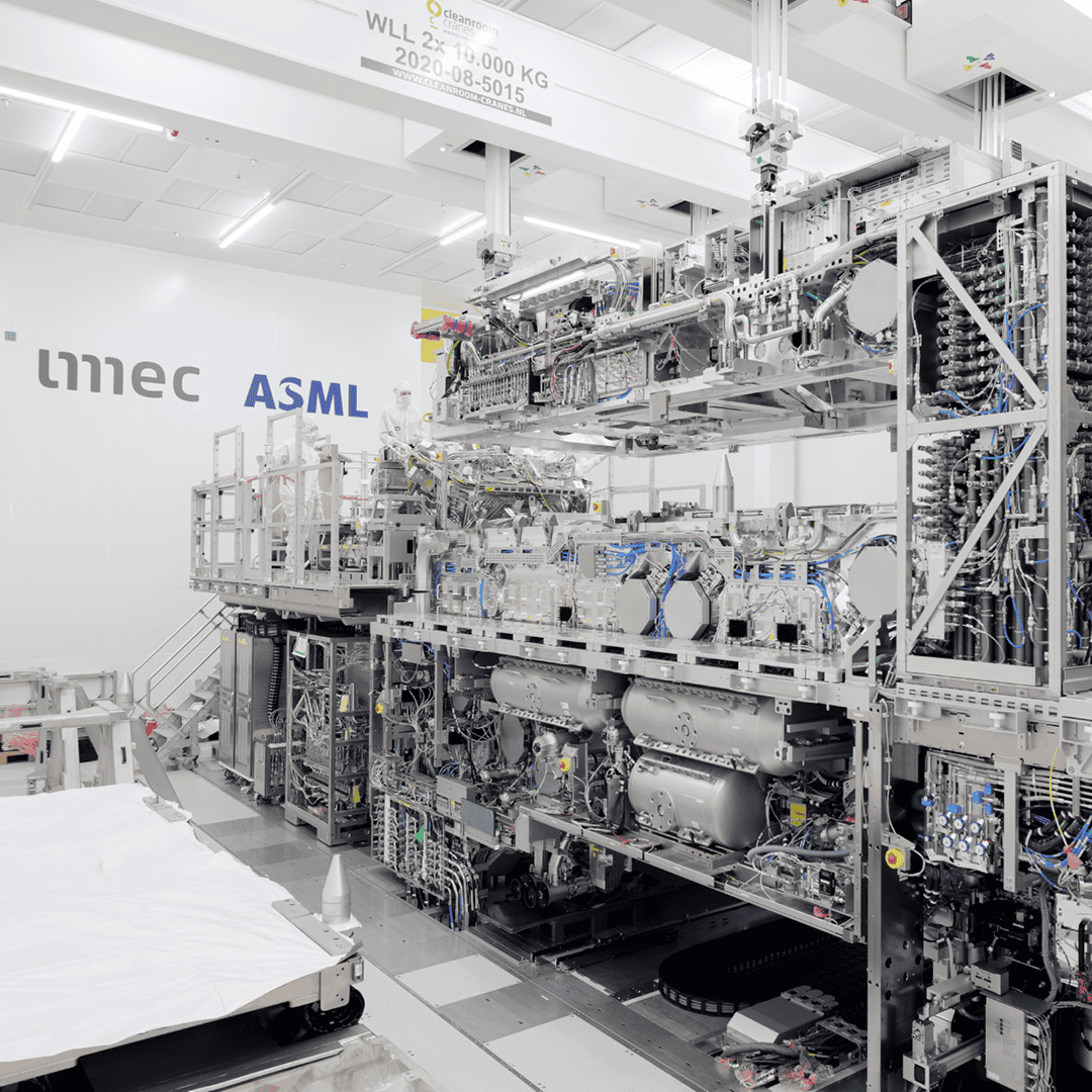
The collaboration between imec and ASML, two pioneers in the chip industry, is not only a technical success but also a strategic move that fits within the ambitions of the European Commission. The European Union strives to strengthen innovation and address societal challenges. ASML’s deployment in imec’s state-of-the-art pilot fab supports this goal by promoting sustainable innovation in Europe.
The memorandum of understanding (MOU) signed by both parties highlights their commitment to working together to develop advanced chip manufacturing technologies. The collaboration between imec and ASML also focuses on preparing this technology for the fastest possible adoption in mass production, which is vital for the future competitiveness of the European chip industry in the global market.
The future in sight
This breakthrough puts imec at the forefront of technological innovation and strengthens Europe’s position in an industry dominated by players from the United States and Asia. The success of this collaboration can serve as a model for future initiatives that strive for technological superiority and sustainable development.
The importance of this development cannot be overstated. It is about more than producing smaller chips; it is about creating the foundation for future innovations that can transform how we live. Imec and ASML have set a new standard that will result in more powerful, efficient, and sustainable technological solutions for decades.