
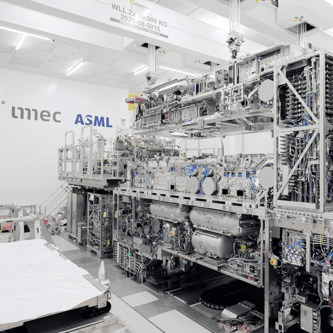
Imec and ASML opened the new High NA EUV Lithography Lab in Veldhoven yesterday. The Lab gives Intel and other leading chipmakers access to the prototype High NA EUV scanner, officially known as TWINSCAN EXE:5000.
Why you should know
Small, smaller, smallest. Those who thought ASML would no longer be able to print even smaller patterns on chips are proven wrong. With the new High NA EUV scanner, the Veldhoven-based company is stretching Moore’s Law even further.
The opening of the joint ASML-imec High NA EUV Lab is a milestone in the preparation of High NA EUV for mass production, expected in 2025-2026. By giving leading manufacturers of logic and memory chips access to the scanner and associated systems, imec and ASML are supporting them in de-risking the technology. This can also help them start designing their own use cases before they get access to these devices themselves.
Starting in 2018
Preparations for the 0.55 NA EUV scanner and infrastructure started back in 2018. In the five years that followed, ASML worked with ZEISS to develop the High NA EUV scanner-specific solutions in the areas of light source, optics, lens anamorphism, stitching, reduced depth of focus, edge placement errors, and overlay accuracy. Meanwhile, imec prepared the patterning ecosystem, including the development of advanced resist and carpet pad materials, photomasks, metrology, and inspection techniques, (anamorphic) imaging strategies, optical proximity correction (OPC), and integrated patterning and etching techniques. All this preparatory work recently resulted in the first exposures with even smaller lineations. For the first time, it succeeded in printing 10 nm dense lines (20 nm pitch) on metal oxide resins (MORs) using the 0.55 NA EUV prototype scanner.

The era of ångström
Imec president and CEO Luc Van den Hove calls High NA EUV “the next milestone” in optical lithography. “It promises patterns of metallic lines with 20 nm pitch in a single exposure and enables the next generations of DRAM chips. This will improve yield and reduce cycle time and CO2 emissions compared to existing multi-patterning 0.33 NA EUV systems.” According to him, this machine will be an essential factor in pushing Moore’s Law “well into the era of ångström.” For imec and its partners, the High NA EUV Lithography Lab will act as a virtual extension of the 300 mm cleanroom in Leuven, further enhancing the patterning ecosystem.
According to ASML’s President and CEO Christophe Fouquet, the Lab can accelerate the technology’s learning curve and smooth its introduction into production. “The ASML-imec High NA EUV Lithography Lab allows our EUV customers, partners, and suppliers to access the High NA EUV system for process development while waiting for their system to be available in their plants. This kind of very early involvement in the ecosystem is unique.”


