
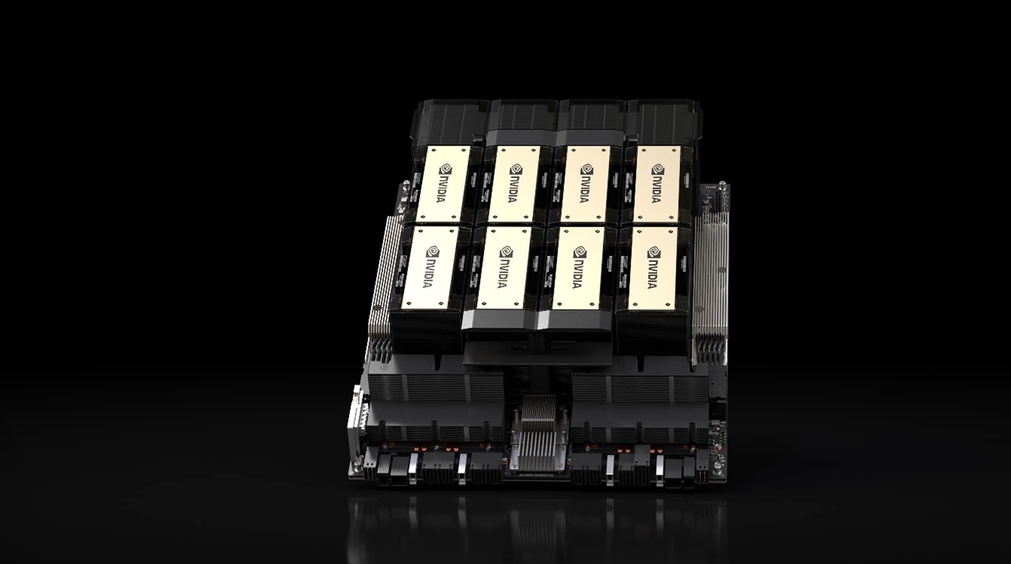

NVIDIA has announced the launch of its new H200 chip, set to supercharge AI and high-performance computing (HPC) workloads. Outpacing its predecessor, the H100, the H200 boasts 1.4x more memory bandwidth and 1.8x more memory capacity, providing an unprecedented performance leap. Availability is expected in the second quarter of 2024, with Amazon, Google, Microsoft, and Oracle among the first to use the new GPUs. The H200’s debut is highly anticipated amidst the high demand for NVIDIA’s chips, which have become so sought-after that they’re being used as collateral for loans. The H200 is not just faster but also more efficient, making it ideal for processing large quantities of data for AI applications.
The vanguard of AI hardware: NVIDIA’s H200 chip
With the advent of the H200, NVIDIA escalates the capabilities of AI and HPC workloads to new heights. The H200 chip is poised to become a cornerstone in the AI technology landscape, heralded for its advanced memory system and capacity to manage more data, enabling the training of larger, more complex models. This leap forward is not just a technical upgrade but also a strategic move to cement NVIDIA’s position in the fiercely competitive AI chip market.
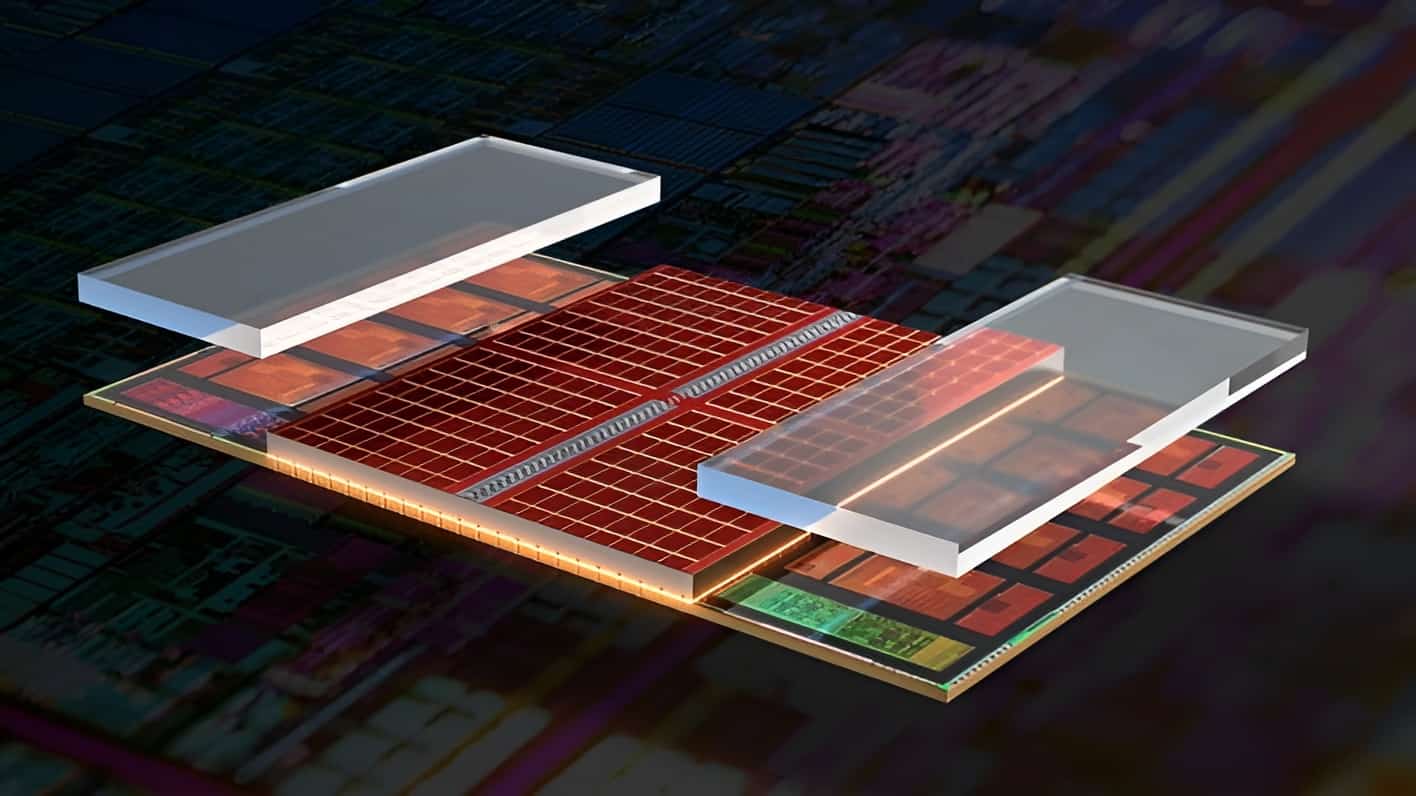
The H200 is not merely an iteration of its forerunners but a significant overhaul. The chip’s technical prowess is underpinned by its new memory system, the HBM3e, which offers a stark improvement over the previous generation. This new form of memory allows for 141 gigabytes of high-bandwidth storage and a data transfer rate of 1.2 terabytes per second, a substantial increase that directly translates into accelerated AI model training and execution.
Anticipated market impact
The introduction of the H200 is expected to exert considerable pressure on NVIDIA’s competitors. The high-end chip market has been dominated by NVIDIA, but AMD and others have been gearing up to challenge this supremacy. With the H200’s advancements, NVIDIA not only upholds its lead but also raises the bar significantly, potentially influencing its market share and competitive stance. The strategic implications of the H200’s capabilities could well echo through the industry, reinforcing NVIDIA’s stronghold, especially as AMD seeks to make inroads with its own AI accelerator chips.
AMD’s efforts to dethrone NVIDIA involve strategic partnerships and technological advancements that aim to disrupt the GPU giant’s hold on the market[8]. With NVIDIA’s H200 on the horizon, the competitive landscape is set to intensify. This rivalry underscores the high stakes in the burgeoning AI chip market, which is forecast to grow from $17 billion in 2022 to a staggering $227 billion by 2032. NVIDIA’s move to a one-year release pattern for its chips, driven by the high demand for its GPUs, is a clear indication of the company’s strategic agility and commitment to maintaining its market dominance.
Technical innovations and AI acceleration
The H200’s technical innovations are not just incremental but transformative. Its architecture represents a significant leap from the H100, with increased memory bandwidth being a key factor in the claimed performance improvements. This advancement is crucial for AI applications where the efficiency of data processing can make or break the viability and speed of model training and inference. As companies like OpenAI push the boundaries of large language models, the need for more powerful hardware becomes paramount. The H200’s ability to handle such demanding tasks nearly doubles its speed compared to the H100, according to tests using Meta’s Llama 2 large language model.
The arrival of the H200 is set to be a boon for AI development. Its superior memory and processing capabilities are expected to alleviate bottlenecks that have constrained the progress and deployment of AI models. NVIDIA’s chips are critical for services like OpenAI’s ChatGPT and a plethora of generative AI services that require rapid and extensive data processing. The H200’s enhanced memory and faster connections to its processing elements suggest these services will be able to deliver responses with greater speed and efficiency.
HBM3e memory: a closer look
The H200’s distinguishing feature, HBM3e memory, signifies a quantum leap for AI hardware. This high-performance memory technology utilises 1β DRAM process technology and sophisticated packaging to achieve industry-leading performance, capacity, and power efficiency. With the ability to store 24GB per 8-high cube and facilitate data transfers at an impressive rate of 1.2TB/s, HBM3e is integral to the H200’s capability to process the vast amounts of data required for cutting-edge AI applications.
Looking towards availability and adoption
Prospective users of the H200 will have to exhibit patience, as the chip is slated for release in the second quarter of 2024. Cloud service behemoths such as Amazon Web Services, Google Cloud, Microsoft Azure, and Oracle Cloud Infrastructure are poised to be among the first to deploy H200-based instances, indicating a broad industry uptake upon release. The H200 chips are expected to command a premium price, similar to their predecessors which cost between $25,000 and $40,000.
Related Posts


