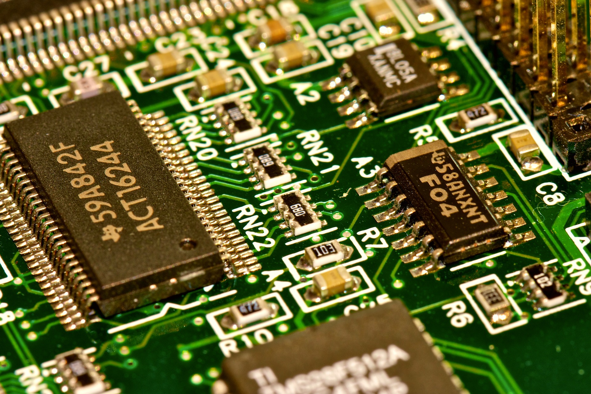
Semiconductors dominate our everyday lives. They form the basis for electronics in computers and cell phones and contribute significantly to optoelectronics through lasers and light-emitting diodes. A decisive factor for the use of semiconductors is the possibility of limiting their dimensionality and thus the free movement of charges – first from three to two, and then further down to one and zero dimensions.
In zero-dimensional structures, also called quantum dots, electrons confined therein have discrete energy values, similar to electrons in atoms. Therefore, quantum dots are often called artificial atoms. Prof. Manfred Bayer, physicist and rector of the Technical University of Dortmund, Germany, together with international researchers, has now identified further potential applications for quantum dots in semiconductors.
Televisions
The development of quantum dots began in the mid-1980s. Two different processes were established for their production. One is physics-based in a high vacuum (epitaxial quantum dots), the other is chemistry-based by synthesis in appropriate solvents (colloidal quantum dots). Both processes quickly found their way into applications: epitaxial quantum dots are used, for example, in quantum dot lasers, while colloidal quantum dots are used as “color converters” to generate the colors green and red in televisions. Researchers have recently made major advances that enable further applications, especially in the production of quantum dots.
The article, written by experts from Toronto, Chicago, Los Alamos, Tokyo, Barcelona and Dortmund, discusses the prospects and problems of such applications. It was recently published in the leading scientific journal Science. It discusses a variety of possible applications for such zero-dimensional structures.
Energy
Colloidal quantum dots could revolutionize photovoltaics, for example, by being embedded in windows. To do this, they would have to be designed to allow light in the visible range to pass through them so that the rooms would still be lit. In contrast, they must absorb light in the infrared range to be converted into electrical energy. This can be achieved by a suitable choice of material and size of quantum dots. In this way, all window facades in high-rise buildings could be used for photovoltaics, for example. The technology could also be used to channel sunlight in greenhouses so that crops can ripen and be harvested more quickly.
Also interesting: Quantum neural networks push machine learning and AI (German only)
The researchers list a number of other applications in the article. These relate to very different fields of technology, such as the production of energy-efficient displays and lighting modules for optoelectronics, sensor technology such as in thermal imaging cameras, the field of quantum technologies or use as medical markers.
In many areas, the applications appear to be within reach. In others, however, significant challenges remain to be solved – be it the development of environmentally-friendly materials without heavy metals, the resource-saving, “green” production of quantum dots using novel chemical raw materials or their recycling.
Original publication: García de Arquer et al.: Semiconductor quantum dots: Technological progress and futurechallenges. Science 373, DOI


