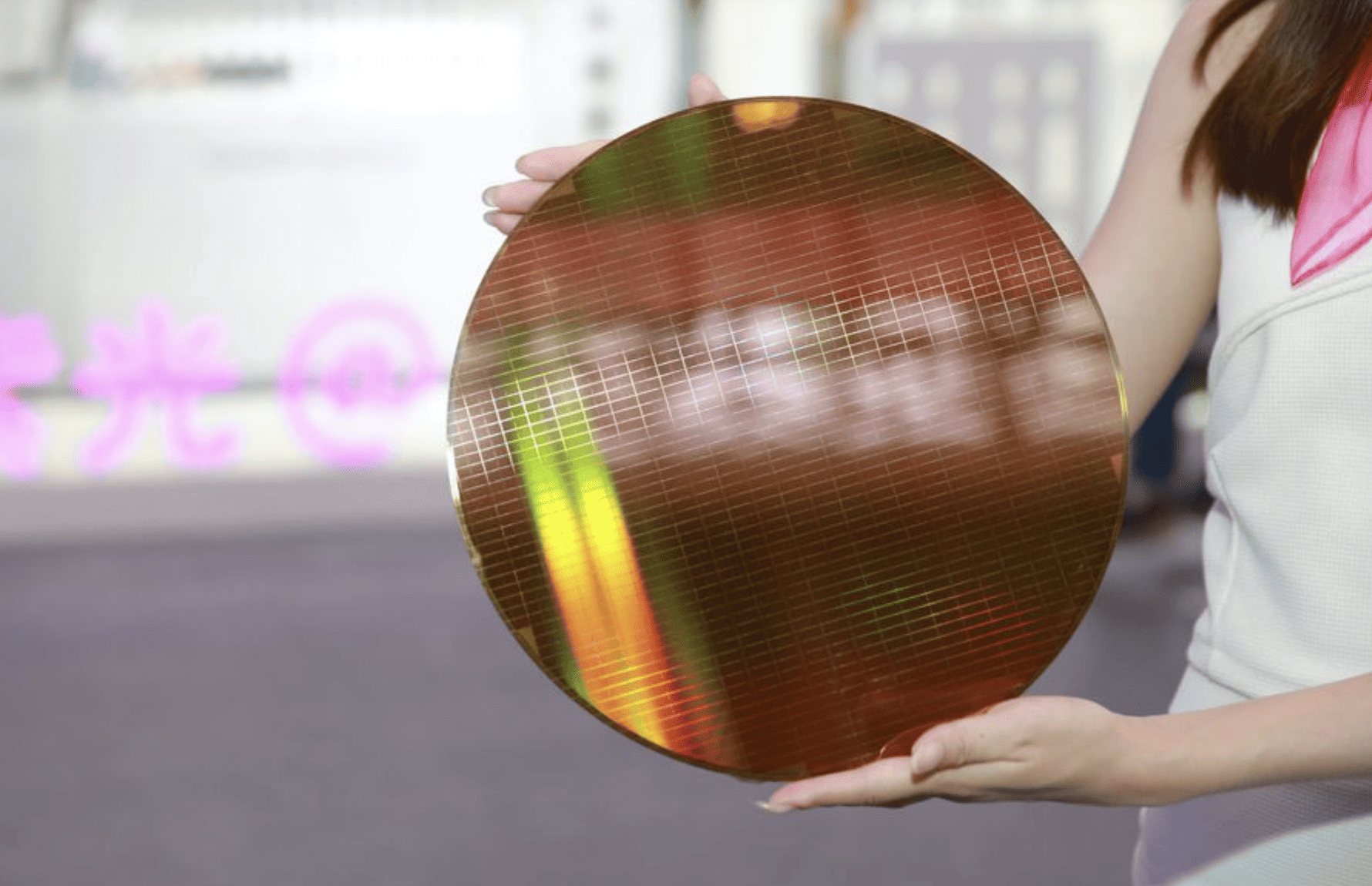
Chinese memory chip producer Yangtze Memory Technologies Co (YMTC) has taken a significant technological leap, creating what is being hailed as the world’s most advanced 3D NAND memory chip. This surprise step, first reported by TechInsights, comes despite YMTC being on the US Commerce Department’s blacklist. The chip, found in a consumer device, marks a notable achievement in China’s ambitions to build its own domestic semiconductor supply chain. This progress is based on YMTC’s new ‘Xtacking 3.0’ architecture and a secret project known as Wudangshan. However, questions remain about the origin of the tools and components used and the upcoming stricter restrictions on lithography systems sales to China.
Defying the odds
The manufacture of this chip by YMTC is striking because it comes against a backdrop of US sanctions. The company, along with 21 other major Chinese players in the chip sector, was added to the US Entity List in December 2022. This list essentially blacklists firms from conducting business with American companies, thereby cutting them off from essential equipment and components. Nonetheless, YMTC continued to develop advanced technology in defiance of these limitations.
Moreover, this isn’t the first time a Chinese tech company has surprised industry insiders. A similar achievement was the Kirin 9000S 5G processor, housed in the Huawei Mate 60 Pro smartphone and produced by SMIC. This processor, which faced its own US restrictions, defied expectations with its performance and features. Therefore, YMTC’s recent success story is part of a broader narrative of resilience and innovation in China’s tech industry in the face of international challenges.
On Wednesday, Bloomberg released a report citing unnamed sources that said SMIC had used retooled equipment from ASML, specifically its deep ultraviolet (DUV) lithography systems, to manufacture the advanced processor in the landmark Huawei smartphone.

Challenging global rivals
The memory chip, a 232-layer X3-9070, was found in a solid-state drive launched quietly in July. Despite some obstacles in its mass production, the chip represents a significant milestone in YMTC’s ambition to compete with memory chip giants like Samsung Electronics, SK Hynix, and Micron Technology. This advancement has enabled YMTC to edge closer to its rivals, with Micron also aiming to start mass production of its 232-layer chip by the end of this year and SK Hynix having developed its first 238-layer memory chip.
Yet, even with this progress, YMTC’s market share remains in the single digits. However, the company is aggressively expanding its production capacity and R&D with the help of state subsidies, and its revenue has improved over the years.

Significance of the chip
The 3D NAND memory chip is pivotal in high-performance computing applications, particularly in artificial intelligence (AI) and machine learning. The chip produced by YMTC is the world’s first quad-level cell (QLC) 3D NAND die with over two hundred active word lines, and it has the highest bit density seen in a commercially available NAND product at 19.8 Gb/mm2. This achievement is significant as it represents the bleeding edge of memory chip design, crucial for high-performance, high-bandwidth computing such as AI.

Upcoming challenges
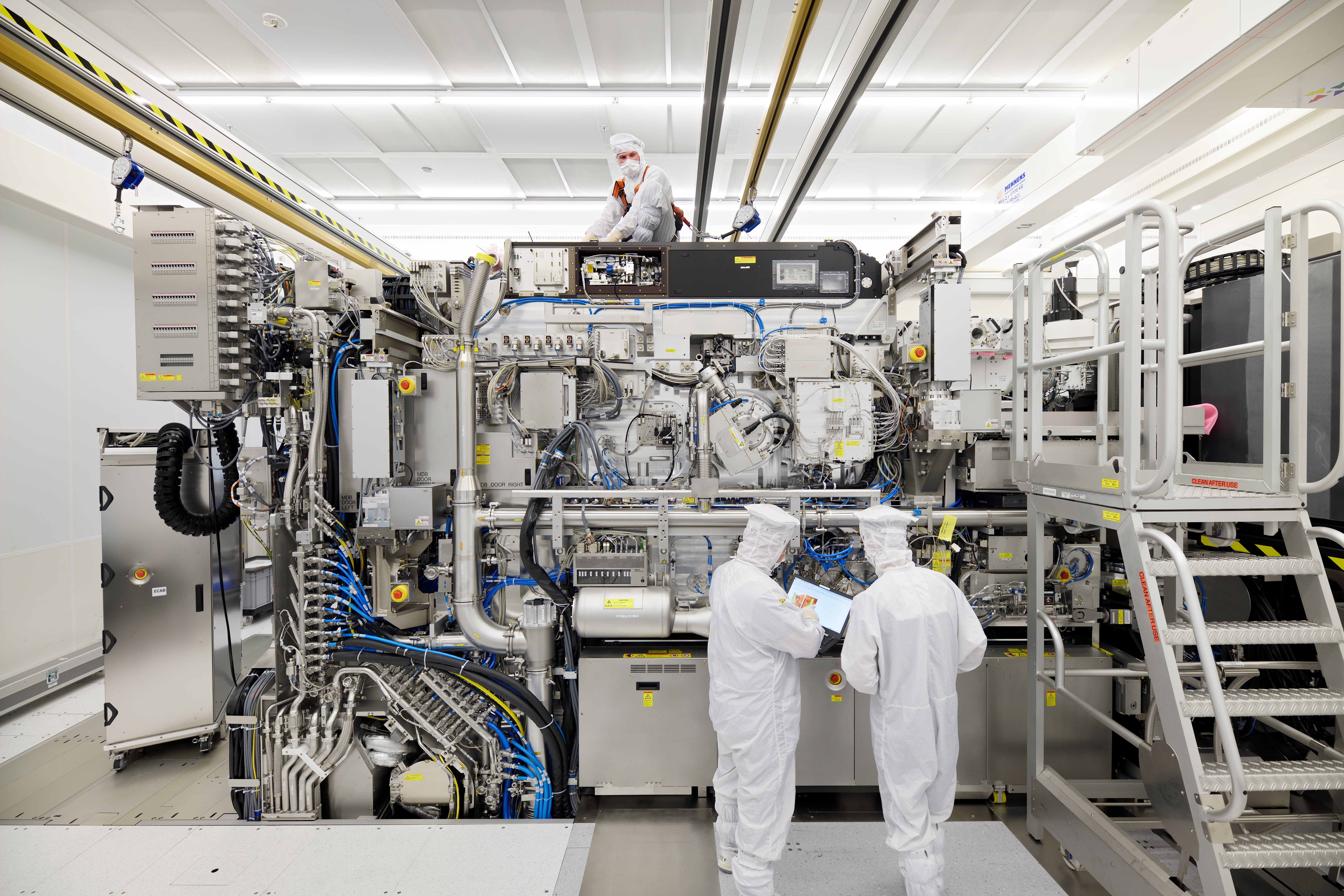
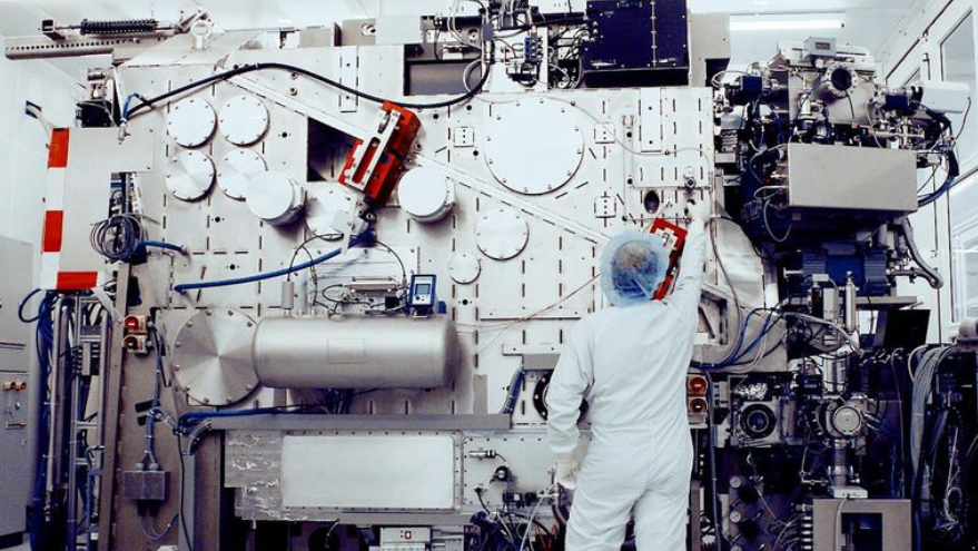
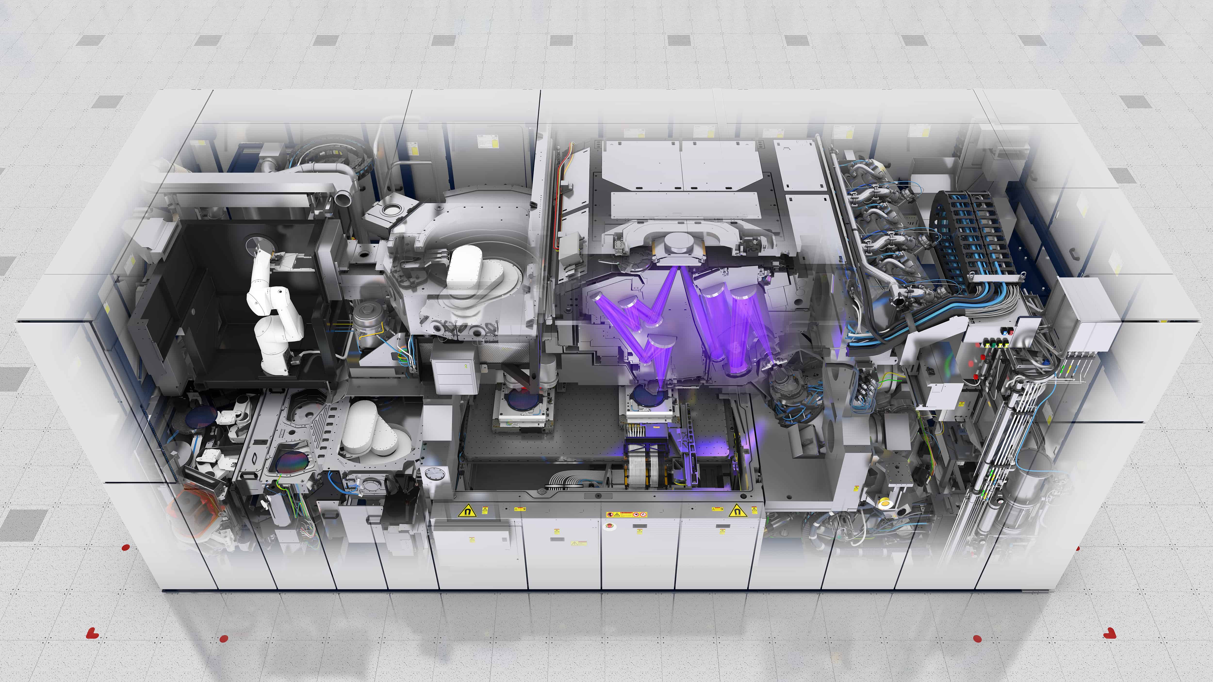
Despite this technological milestone, the future for YMTC, and indeed other Chinese tech companies, is not devoid of challenges. YMTC’s ambitions could be disrupted by the looming stricter restrictions on lithography systems sales to China, set to be implemented in January 2024. ASML, a company that produces lithography systems, has been prohibited from selling its advanced EUV lithography systems to China since 2019, and the upcoming restrictions will prevent ASML from selling its 2000-series DUV machines as well. Chinese firms still lag in producing the necessary lithography systems to progress significantly.


