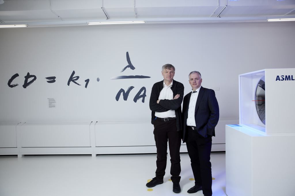
With their method of etching geometric patterns on silicon wafers, ASML’s inventors Erik Loopstra and Vadim Banine were awarded the Popular Prize of the European Inventor Award 2018. The Award ceremony held today in Paris, Saint-Germain-en-Laye, was attended by some 600 guests from the areas of politics, business, intellectual property, and science. The two inventors and their teams at ASML and Zeiss developed an extreme ultraviolet lithography (EUVL) production system for smaller, faster and more powerful semiconductors.
“The public vote for Erik Loopstra and Vadim Banine honours their contributions to helping chart the future of computer-chip production,” said President Benoît Battistelli of the Munich based European Patent Office (EPO). “Smaller, more powerful microchips will likely drive developments in fields ranging from consumer electronics to autonomous driving and Artificial Intelligence. We can see how European advances in chip technology can have a big impact on the digital economy.”
Loopstra and Banine received the most public votes from among the thousands cast online. Awards were also handed over to winners in the categories “Industry”, “Small and medium-sized enterprises (SMEs)”, “Research”, “Non-EPO countries” and “Lifetime achievement”, as chosen by the international jury from more than 500 individuals and teams of inventors put forward for this year’s Award.
The European Inventor Award is presented annually by the EPO to recognise outstanding inventors from Europe and around the world who have made an exceptional contribution to social development, technological progress, and economic growth.
Moore’s Law extended
Ever smaller, more powerful chips are critical to further technological developments of the digital age. Following a prediction made by US engineer and Intel Corporation co-founder Gordon Moore, computing power has roughly doubled every two years since the 1960s. However, conventional chip manufacturing methods have approached their physical and economic limits – signalling a possible departure from Moore’s Law and a slowdown in technologies across numerous related fields. Helping extend Moore’s Law into the future, Loopstra, Banine and their teams developed an EUVL production system that reduces the wavelength of the radiation used to etch chip details by a factor of 14.
“With a wavelength almost as short as X-ray, we image features on the chip of only 5 nanometers wide, which is barely 20 silicon atoms,” explains Vadim Banine. “With this technology, we’ve almost reached the limits of conventional physics.”
The EUVL system aims a high-powered laser to heat tiny droplets into plasma and generate extreme ultraviolet radiation that is then directed through highly precise optics onto a chip’s silicon substrate for etching tiny chip details. “Optics are no longer made of lenses, but by the world’s smoothest mirror system,” says Erik Loopstra. He notes that if one of the EUVL system’s mirrors were expanded to the size of Germany, or 1 000 km across, the greatest deviation would be less than the width of a human hair. In addition to advanced optics and high-powered laser, the EUVL system features a vacuum environment developed by the inventors and their team that reduces contamination – caused by lumps of material 1 000 times thinner than a human hair – to almost zero.
The two inventors point to the role that patents have played in securing important intellectual property protection. “Only if you put your ideas into patents, can you have the freedom of operation,” says Loopstra. “Even if somebody else has the same idea later, you can keep on working
on your own invention.”

