World Economic Forum (WEF) asked a group of international technology experts to identify this year’s Top 10 Emerging Technologies. After soliciting nominations from additional experts around the globe, the group evaluated dozens of proposals according to a number of criteria. Do the suggested technologies have the potential to provide major benefits to societies and economies? Could they alter established ways of doing things? Are they likely to make significant inroads in the next several years? “Technologies that are emerging today will soon be shaping the world tomorrow and well into the future – with impacts to economies and to society at large”, said Mariette DiChristina, Editor-in-Chief of Scientific American, and chair of the Emerging Technologies Steering Committee. In our constant lookout for the origins of innovation, IO will present WEF’s top-10 emerging technologies in a 10-part series. Today: Tiny lenses.
After part 10 has been published, the whole series can be found here
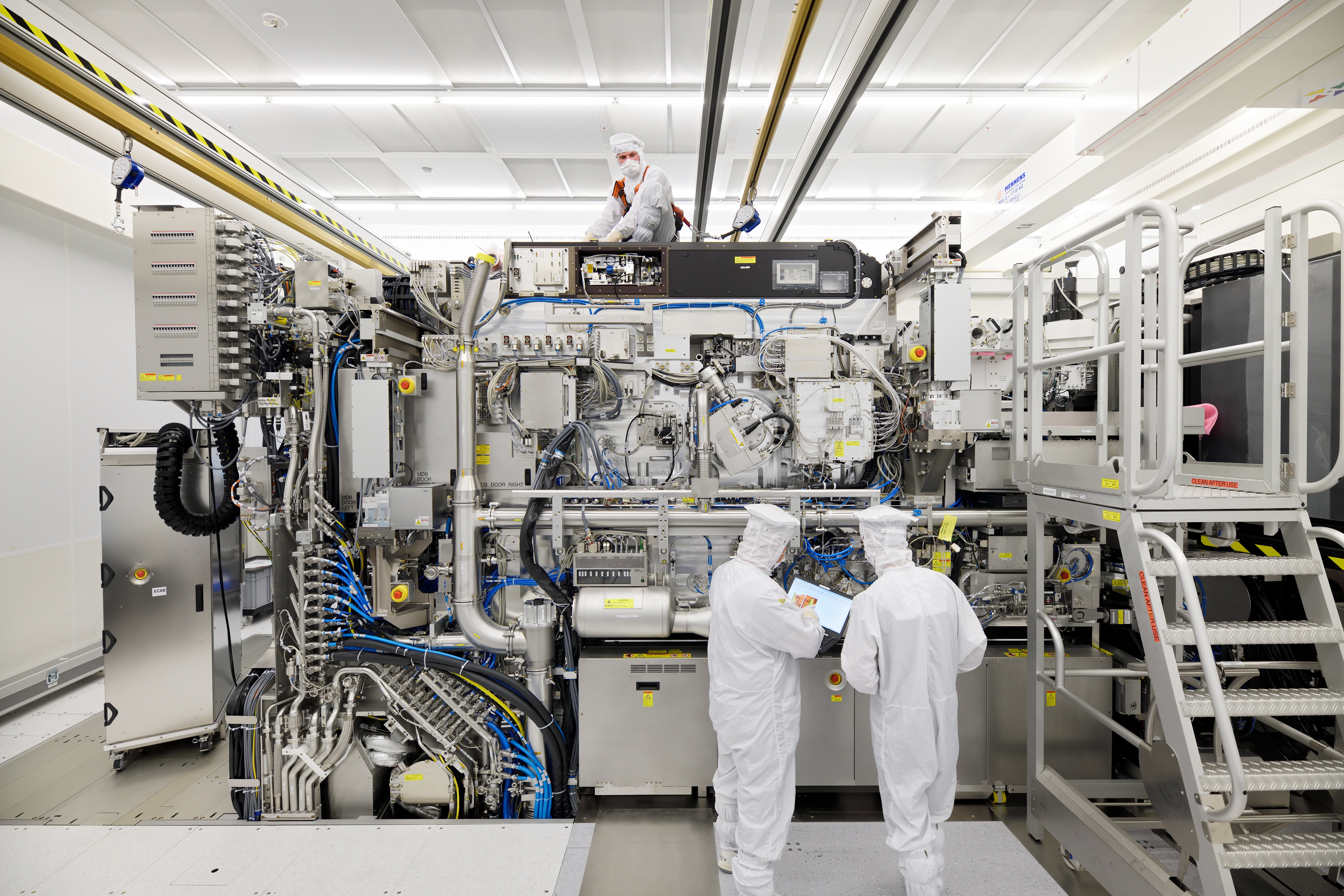
Semiconductor giants like ASML are built upon Moore’s Law and perfect optical solutions like Zeiss’ lenses. But as phones, computers and other electronics have grown ever smaller (Moore said so!), their optical components have stubbornly refused to shrink, the WEF-researchers observe. “Notably, it is hard to make tiny lenses with traditional glass-cutting and glass-curving techniques, and the elements in a glass lens often need to be stacked to focus light properly.” Still, engineers have recently figured out much of the physics behind much smaller, lighter alternatives known as metalenses. These lenses could allow for greater miniaturization of microscopes and other laboratory tools, as well as of consumer products, such as cameras, virtual reality headsets and optical sensors for the internet of things. And they could enhance the functionality of optical fibres.
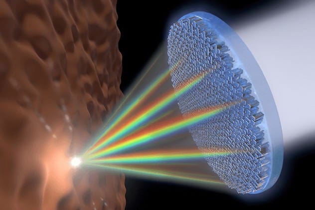
A metalens consists of a flat surface, thinner than a micron, that is covered with an array of nanoscale objects, such as jutting pillars or drilled holes. As incident light hits these elements, many of its properties change – including its polarization, intensity, phase and direction of propagation. Researchers can precisely position the nanoscale objects to ensure that the light that exits the metalens has selected characteristics. What is more, metalenses are so thin that several can sit on top of one another and still be tiny in size.
Expenses
There’s another advantage to metalenses. In addition to reducing the size, metalenses should ultimately lower the cost of optical components because the diminutive lenses can be manufactured with the same equipment already used in the semiconductor industry. “This feature raises the alluring prospect of fabricating, say, a tiny light sensor’s optical and electronic components side by side.”
For now, however, expenses are still high because it is difficult to precisely place nanoscale elements on a centimetre-scale chip. Other limitations also need addressing. So far, metalenses do not transmit light as efficiently as traditional lenses – an important capability for such applications as full-colour imaging. In addition, they are too small to capture a large quantity of light, which means that, for now, they are not suited to snapping high-quality photographs.
Nevertheless, the WEF researchers are convinced that in the next few years, the tiny lenses will make their way into smaller, easier-to-manufacture sensors, diagnostic tools such as endoscopic imaging devices, and optical fibres. “Those potential applications are appealing enough to have attracted research support from government agencies and such companies like Samsung and Google. At least one start-up, Metalenz, expects to bring metalenses to market within the next few years.”
(Most of this article is drawn from the 2019 Top 10 Emerging Technologies report)


