

MBraun’s representative looks pleased as he watches his “Glove Box” being used in practice. It has large glass cabinets with rubber arms to allow the employees of the Helmholtz Zentrum Berlin (HZB) to work in a sterile environment. A young researcher is mirroring two solar cells on top of each other in one of the cabinets, “because that’s one of the things we do here”, says HZB professor Steve Albrecht. “Together with our partners, we are looking for new applications in the photovoltaic industry.”
The “Industrietag 2019” in the HZB research centre in the Berlin district of Adlershof provides a perfect opportunity to showcase the most promising projects to colleagues from the industry and other scientific institutes. Amongst them are members of the renowned Max-Planck Institute and Fraunhofer, but also companies such as Von Ardenne and Oxford PV.
Merkel and the Wright brothers
The majority of them work within walking distance, because in Adlershof a great deal of photovoltaic knowledge is concentrated in a relatively small area of 4.1 km2. “It is no coincidence that this district has been an industrial research centre since the beginning of the last century,” explains Roland Sillmann of Wista Management, the organisation that has a major say in who is allowed to set up business in Adlershof.

Sillmann: “This is the location of one of the first German airports at the beginning of the twentieth century. The Wright brothers, amongst others, tested their planes here. In the 1920s, one of BMW’s most important factories was located here, and in the GDR period, it was the most important research centre. And did you know that Angela Merkel studied here?”
After the fall of the Wall in 1989, it took some time for Adlershof to get back on its feet, but now, according to Sillmann, it is once again one of the most important technology centres in Germany. It is home to 16 scientific institutions and 1,150 companies, most of them active in the fields of renewable energy, nanotechnology and fabrication, biotechnology and the optical industry.
Thin-layer composites
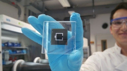
HZB conducts research in various domains in the field of solar cells. They are experimenting with the traditional silicon as a semiconductor material, but other materials are also very important, such as the so-called thin-layer composites CIGS (copper, indium, gallium and selenide) and the mineral perovskite. These provide a much higher efficiency and are generally thinner.
According to Rutger Schlattmann, who is responsible for communicating scientific knowledge to companies at HZB, one of the most promising projects is the combination of perovskite and CIGS solar cells, a study that is being carried out in cooperation with the Eindhoven University of Technology.
Tandem cells
“The great advantage of these “tandem cells” is that perovskite can convert blue light from the sun into energy, while CIGS cells target the red spectrum,” explains Schlattmann. When combined, this results in extra powerful cells which can eventually convert up to 30% of the sunlight into electricity, he believes. By comparison, the average rooftop solar panel has an efficiency of between 15 and 20%.

HZB has now reached an efficiency of 21.6% with its “perovskite CIGS cells”, according to Professor Albrecht. It is more or less at the same level as European research centre Solliance, which recently reached 21.5%. The centre, based in Eindhoven, also sees great opportunities in this technology.
HZB has another tandem solar cell with an even higher efficiency of over 25%, which is composed of perovskite and silicon. For these tandem solar cells, it has already built an industrial pilot plant in Brandenburg, in collaboration with British company Oxford PV. According to Schlattmann, the main advantage of the perovskite CIGS solar cells is that they are much cheaper to produce, both due to lower material costs and lower energy consumption. However, this requires the transition from laboratory to industrial application, which is often the most difficult step.
Related Posts


