

ZEISS Oberkochen celebrated “50 Years of Enabling the Semiconductor Industry”
No, the 7-nanometer chips in the new iPhones are not produced in one of ASML’s EUV chip machines. But it won’t be long before the first commercial EUV-enabled chips will hit the market. Veldhoven based ASML and Oberkochen based partner Zeiss expect this to happen early next year.
At the Zeiss celebration of ’50 Years of Enabling the Semiconductor Industry’ held in Oberkochen last week, Dr. Martin van den Brink, President and CTO of ASML, highlighted the way in which EUV lithography has helped shape the microelectronics industry: “The launch of EUV in chip fabs around the world was based on major scientific efforts and technological innovation. The fourth generation of the EUV system, the NXE:3400B, is currently rolled out in the mass production processes at several customers.” The first generation of chips based on EUV lithography will be launched early next year – and ASML is already working on the next lithography platform: EUV with high numerical aperture. Van den Brink: “This system will enable geometric chip scaling beyond the next decade and offer 70% better resolution and positioning accuracy than the most advanced EUV systems available today.”
First lens for a circuit board exposure device
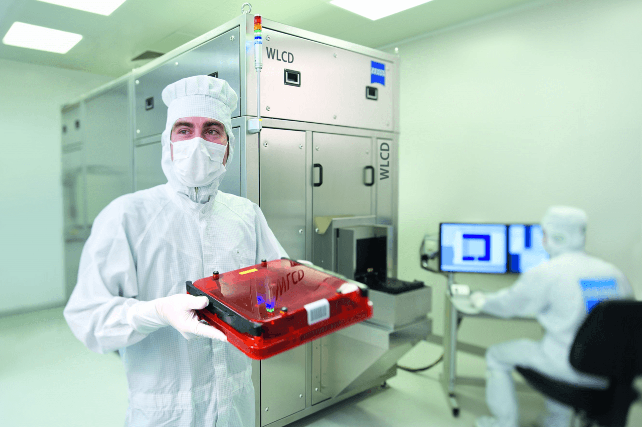
In 1968, ZEISS supplied a lens for a circuit board exposure device for the first time. At the time, the predecessor of today’s wafer scanners for chip production mapped structures of more than ten micrometres. Today, ZEISS Semiconductor Manufacturing Technology (SMT) lithography optics with extreme ultraviolet light (EUV) already enable structures of less than 20 nanometers. Used in the wafer scanners of strategic partner ASML, they enable the production of increasingly powerful, smaller, cheaper and more energy-efficient chips. They pave the way for microelectronic innovations such as the Internet of Things, Smart Production, electromobility and self-driving cars.
EUV lithography as a model for European cooperation
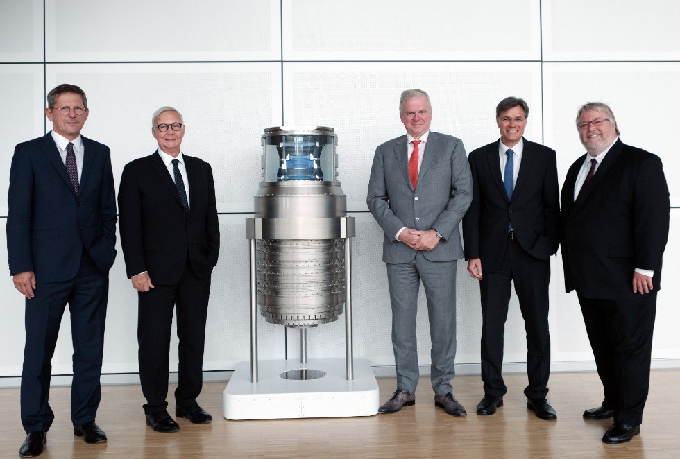
The 50-year development of semiconductor manufacturing technologies from ZEISS and the lithography systems developed by ASML since 1984 have culminated in the production of EUV lithography in 2018. The success of EUV technology is a model for European cooperation in research, industry and politics, Zeiss says. The German government, the Dutch government and the European Commission have all been promoting research and development in lithography for around three decades. The aim of the ZEISS event “50 Years of Enabling the Semiconductor Industry” held in Oberkochen was to celebrate what has been achieved together with sponsors, project partners and stakeholders, as well as to discuss the future of successful cooperation in strategy discussions.
Dr. Georg Schütte, State Secretary at the Federal Ministry of Education and Research (BMBF), emphasized the importance of long-term funding: “We will continue to strengthen the position of microelectronics in Germany with the new High-Tech Strategy 2025. We are convinced that technological sovereignty is a valuable commodity today. ZEISS and ASML are a fine example of how Europe can conduct excellent research and produce innovations. The keys to success were European cooperation and ongoing public funding.” Since 2005, the BMBF has invested a total of €900 million in microelectronics.
Moore’s Law
The EUV systems – with an exposure wavelength of 13.5 nanometers – enable finer chip structures than classic lithography systems. “This technological leap is the biggest in the history of chip manufacturing and continues Moore’s law“, a Zeiss spokesperson said. “This is crucial in semiconductor electronics, and states that the number of integrated circuits that can fit on a microchip will double every two years.”
More on Moore’s Law – or look at this statement by Maarten Steinbuch:
“If I look at the developments at ASML, Moore’s prediction will certainly continue for about thirty to forty years. I base this, among other things, on the current immersion lithography, which has not yet been developed fully. The company is also moving forward with EUV technology. The next step is optical computers, or photonics, followed by quantum computing.”
(Photo (c) BertPauli.nl)
Related Posts


