

EFFECT Photonics, located in the Videolab at Strijp-S in Eindhoven, announced earlier this week that it had completed a new financing round. Reason for an interview about the current status and goals.
“This is the perfect time to take our product to market,” says Joost Verberk, director of PLM (Product Line Management) at EFFECT Photonics. “Not many people are aware of this, but the increasing demand for Netflix and YouTube, for example, costs a huge amount of energy. Currently, four or five per cent of energy consumption goes to all data centres in the world. If we don’t change something about the current technology, we will need one hundred per cent of the current capacity in 2030 just to keep the internet going. That is not possible. Our technology is a solution because it is a more energy-efficient way to meet that demand.”
Much more about Photonics on Innovation Origins
Autonomous cars and virtual reality

Within EFFECT Photonics, Verberk is the link between the customer and the technical team. He travels all over the world to hear what is going on in the market and what customers need. Early this year he was in Barcelona for the Mobile World Congress. “That’s where you actually look into the future of telecom for six months to perhaps a year. The buzzword was: 5G. That is going to change so much and it will make many new applications possible. It’s enabling autonomous cars and virtual reality applications. But for that to happen, a lot needs to be done in the network. Our products fit precisely into this development.”
It’s always difficult to tell this story in simple English, says Verberk. Yet he keeps trying. “It’s a super complicated technical product. Yes, it makes the internet of the future possible, but it is difficult to explain why it is so good or why you should use it.”
Fortunately, customers of EFFECT Photonics see the benefits and understand that. “They know what we’re talking about; they know the technology and material properties. They see the possibilities of our basic material.”
An immature market
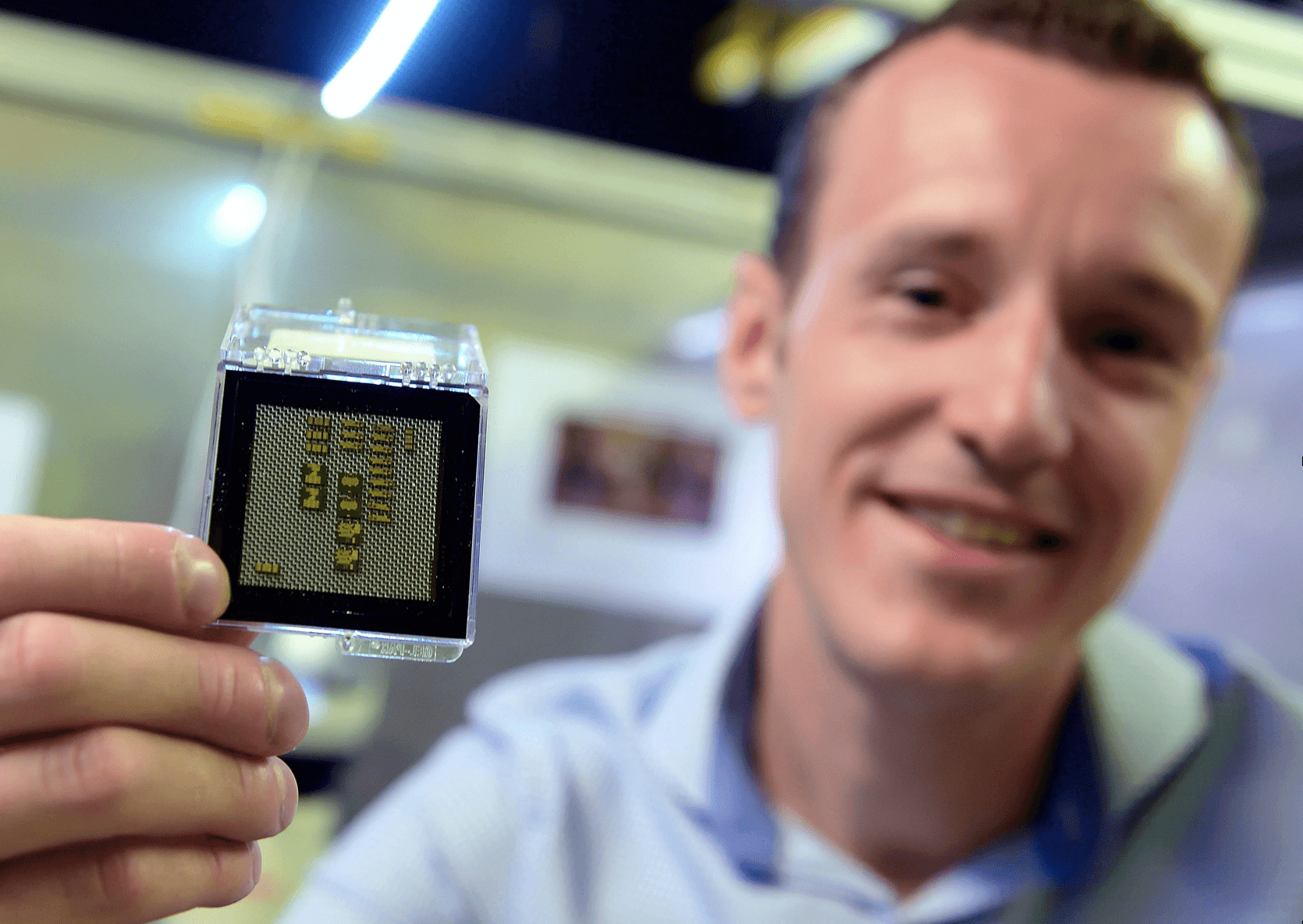
EFFECT Photonics makes so-called ‘Photonic Integrated Circuits’: integrated photonics on a chip. All optical elements come together on one chip. They are the only ones in the world to do so. To do this, they use the basic material indium phosphide. Normal chips for phones and computers are made of silicon. Both materials form the basis for all the tiny components with which they build the chip. There is a big difference between the two materials: “our chips generate light signals. This is not possible in silicon but in indium phosphide it is.”
“If we don’t change the current technology, we’ll need one hundred per cent of the current capacity in 2030 just to keep the internet going. That’s not feasible”
“What makes it difficult is that it is an immature market, that of silicon is much more mature. We can’t make this product on our own.” And so EFFECT Photonics needs partners to get it done. And money. Because hardware development is expensive, says Verberk. Four years ago EFFECT Photonics held a first investment round and now the company has just completed the second one. “It just takes a lot of money, tens of millions, to bring a product to the market. And then you need long-term investors.”
A prerequisite for an investor is that he understands that it is long-term work. “That they know what it is like to get into a hardware technology start-up. They can’t expect to get all their money back next year. What helped in finding investors in the first round was that the CEO, James Regan, and the VP-sales & marketing, Robert Hughes, came from the telecom world and had their contacts there.
An R&D office at the Torenallee in Eindhoven
“The use of indium phosphide is completely new. We need to do a lot of research to test if it works. That testing takes time.” This is different when developing software, for example. “With an app, you press ‘compile’ and a few minutes later you know if it works. With us, it takes six months to know whether our design works.”
The R&D office is on the Torenallee in Eindhoven. There is a separate ‘test room’, a kind of cleanroom, but you don’t have to wear a coat ‘if you don’t touch anything’. It’s buzzing with equipment and air conditioners. “These chips contain a lot of building blocks such as very small lasers and photodiodes that combine the light. We measure all these building blocks. How much light comes from a laser and how much power should you put in it? What happens if you make it a micrometre larger, do you get more light out of it for the same amount of current?”
Their real cleanroom is in England, Brixham, where 25 people work on assembling the chips into modules. Eindhoven employs 40 people from 15 different nationalities. By the end of this year, EFFECT wants to grow to 100 employees.
An international business
 Last month Verberk travelled to America, from America to China and back again to the Netherlands. Next month England and Italy are on the program. “It’s just a very international business. Customers are all over the world.”
Customers? How is that possible, if they have not yet launched the product on the market? “They have bought samples and there are already orders. They evaluate our product and see if it fits in their systems. Whether the performance is what we expect from it. During the previous round of samples, the performance was not good enough. We are now working on the last round. If our customers approve, the volume orders can begin.”
Those customers got enthusiastic thanks to the good contacts of James Regan and Robert Hughes. “And also important: customers are excited about the price. Because we can go far below the price of our competitors. And I really mean tens of percents lower, because we have a much less complex assembly.”
“People believe in technology. This product is actually a means to an end.”
But these are the short-term customers, as Verberk calls them. “Our long-term customers who join our research programmes are particularly enthusiastic about the opportunities offered by the raw material. They are particularly interested in the energy-efficient and high-performance properties. Our entry-level model is actually not as energy-efficient as it could be. And this material can do much faster as well. We want to develop further and then compete on performance.”
1 terabit per second
The first product made by EFFECT Photonics sends 10 gigabits per second. “The really big customers are already thinking about 1 terabit per second. That’s a hundred times faster. They are convinced that this is only possible with indium phosphide integrated chips, so they want to do a research program with us. They find the technology so interesting that they pay us to do part of an applied research program.”
“We’ve been around for seven years now and we’re almost there. We expect to succeed this year. The company is doing well, even despite the fact that we haven’t really put anything on the market yet. People believe in technology. This product is actually a means to an end.”
Much more about Photonics on Innovation Origins
Main picture (c) Brainport Monitor
Side photos: stills from video Omroep Brabant
Related Posts


